
Datasheet


Section 25 Electrical Characteristics
Page 1234 of 1384 R01UH0310EJ0500 Rev. 5.00
Sep 25, 2012
H8S/2426, H8S/2426R, H8S/2424 Group
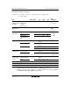
Item Symbol Min. Typ. Max. Unit
Test
Conditions
V
CC
− 0.3 ⎯ ⎯ V I
OH
= −200 μA
V
CC
− 0.5 ⎯ ⎯ V I
OH
= −1 mA
Output high
voltage
All output pins V
OH
V
CC
− 0.8 ⎯ ⎯ V I
OH
= −2 mA
All output pins ⎯ ⎯ 0.4 V I
OL
= 4.0 mA Output low
voltage
P26 and P27*
4
P32 to P35*
4
,
P50 and P51*
4
V
OL
⎯ ⎯ 0.4 V I
OL
= 8.0 mA
RES ⎯ ⎯ 10.0 μA
STBY, NMI,
MD2 to MD0
⎯ ⎯ 1.0 μA
V
in
= 0.5 to
V
CC
−0.5 V
Input
leakage
current
Port 4, Port 9
|I
in
|
⎯ ⎯ 1.0 μA V
in
= 0.5 to
AV
CC
−0.5 V
Notes: Pins of port 2, P32 to P35, P50 and P51, and P81 and P83 are 5-V tolerant.
1. When the A/D and D/A converters are not used, the AV
CC
, V
ref
, and AV
SS
pins should not
be open. Connect the AV
CC
and V
ref
pins to V
CC
, and the AV
SS
pin to V
SS
.
2. When used as IRQ, TIOC, TCLK, TMRI, SCL, or SDA.
3. When used as other than IRQ, TIOC, TCLK, TMRI, SCL, or SDA.
4. When used as SCL or SDA.
5. When used as SSO, SSI, SSCK, SCS, WAIT, ADTRG1 or DREQ.
6. When used as other than SSO, SSI, SSCK, SCS, WAIT, ADTRG1 or DREQ.