
Datasheet


Section 25 Electrical Characteristics
Page 1228 of 1384 R01UH0310EJ0500 Rev. 5.00
Sep 25, 2012
H8S/2426, H8S/2426R, H8S/2424 Group
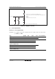
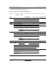
Item Symbol Min. Max. Unit Test Conditions
A/D
converter
Trigger input setup time t
TRGS
30 ⎯ ns Figure 25.46
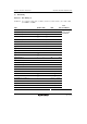
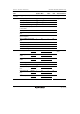
IIC2 SCL input cycle time t
SCL
12 t
cyc
+600 ⎯ ns Figure 25.47
SCL input high pulse width t
SCLH
3 t
cyc
+300 ⎯ ns
SCL input low pulse width t
SCLL
5 t
cyc
+300 ⎯ ns
SCL, SDA input falling time t
Sf
⎯ 300 ns
SCL, SDA input spike pulse
removal time
t
SP
⎯ 1 t
cyc
ns
SDA input bus free time t
BUF
5 t
cyc
⎯ ns
Start condition input hold
time
t
STAH
3 t
cyc
⎯ ns
Retransmit start condition
input setup time
t
STAS
3 t
cyc
⎯ ns
Stop condition input setup
time
t
STOS
3 t
cyc
⎯ ns
Data input setup time t
SDAS
1 t
cyc
+20 ⎯ ns
Data input hold time t
SDAH
0 ⎯ ns
SCL, SDA capacitive load Cb ⎯ 400 pF
SCL, SDA falling time t
Sf
⎯ 300 ns
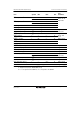
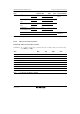
Master 4 256 SSU* Clock cycle
Slave
t
SUcyc
4 256
t
cyc
Figures 25.48 to
25.51
Master 48 ⎯ Clock high pulse
width
Slave
t
HI
48 ⎯
ns
Master 48 ⎯ Clock low pulse
width
Slave
t
LO
48 ⎯
ns
Clock rising time t
RISE
⎯ 12 ns
Clock falling time t
FALL
⎯ 12 ns
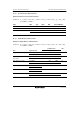
Master 25 ⎯ Data input setup
time
Slave
t
SU
30 ⎯
ns
Master 10 ⎯ Data input hold
time
Slave
t
H
10 ⎯
ns
Master 2.5 ⎯ SCS setup time
Slave
t
LEAD
2.5 ⎯
t
cyc