
Datasheet


Section 25 Electrical Characteristics
R01UH0310EJ0500 Rev. 5.00 Page 1225 of 1384
Sep 25, 2012
H8S/2426, H8S/2426R, H8S/2424 Group
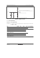
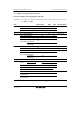
Item Symbol Min. Max. Unit
Test
Conditions
t
OED1
⎯ 15 ns OE delay time 1*
1
t
OED1B
⎯ 19 ns
t
OED2
⎯ 15 ns OE delay time 2*
1
t
OED2B
⎯ 19 ns
Precharge time 1 t
PCH1
1.0 × t
cyc
−20 ⎯ ns
Precharge time 2 t
PCH2
1.5 × t
cyc
−20 ⎯ ns
Figures 25.8 to
25.23, 25. 29
and 25.30
Self-refresh precharge time 1 t
RPS1
2.5 × t
cyc
−20 ⎯ ns
Self-refresh precharge time 2 t
RPS2
3.0 × t
cyc
−20 ⎯ ns
Figures 25.22
and 25.23
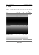
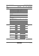
WAIT setup time t
WTS
25 ⎯ ns
WAIT hold time t
WTH
1 ⎯ ns
Figures 25.10,
25.16, and
27.35
BREQ setup time t
BREQS
30 ⎯ ns
BACK delay time t
BACD
⎯ 15 ns
Bus floating time t
BZD
⎯ 40 ns
Figure 25.24
BREQO delay time t
BRQOD
⎯ 25 ns Figure 25.25
Address delay time 2*
2
t
AD2
⎯ 16.5 ns Figure 25.26
CS delay time 4*
2
t
CSD4
⎯ 16.5 ns Figure 25.26
DQM delay time*
2
t
DQMD
⎯ 16.5 ns Figure 25.26
t
CKED
⎯ 16.5 ns CKE delay time*
2
*
3
t
CKEDB
⎯ 19 ns
Figures 25.27
and 25.28
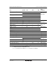
Read data setup time 3*
2
t
RDS3
15 ⎯ ns Figure 25.26
Read data hold time 3*
2
t
RDH3
0 ⎯ ns Figure 25.26
Write data delay time 2*
2
t
WDD
⎯ 31.5 ns Figure 25.26
Write data hold time 4*
2
t
WDH4
2 ⎯ ns Figure 25.26
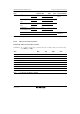
Notes: 1. t
OED1
, and t
OED2
correspond to the OE-A and RD, t
OED1B
, and t
OED2B
correspond to the OE-B.
2. Supported only by the H8S/2426R Group.
3. t
CKED
corresponds to the CKE-A, t
CKEDB
corresponds to the CKE-B.