
Datasheet

Section 24 List of Registers
Page 1198 of 1384 R01UH0310EJ0500 Rev. 5.00
Sep 25, 2012
H8S/2426, H8S/2426R, H8S/2424 Group
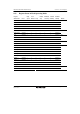
Register
Abbreviation Bit 7 Bit 6 Bit 5 Bit 4 Bit 3 Bit 2 Bit 1 Bit 0 Module
TCR_2 ⎯ CCLR1 CCLR0 CKEG1 CKEG0 TPSC2 TPSC1 TPSC0
TMDR_2 ⎯ ⎯ ⎯ ⎯ MD3 MD2 MD1 MD0
TIOR_2 IOB3 IOB2 IOB1 IOB0 IOA3 IOA2 IOA1 IOA0
TIER_2 TTGE ⎯ TCIEU TCIEV ⎯ ⎯ TGIEB TGIEA
TSR_2 TCFD ⎯ TCFU TCFV ⎯ ⎯ TGFB TGFA
Bit 15 Bit 14 Bit 13 Bit 12 Bit 11 Bit 10 Bit 9 Bit 8 TCNT_2
Bit 7 Bit 6 Bit 5 Bit 4 Bit 3 Bit 2 Bit 1 Bit 0
Bit 15 Bit 14 Bit 13 Bit 12 Bit 11 Bit 10 Bit 9 Bit 8 TGRA_2
Bit 7 Bit 6 Bit 5 Bit 4 Bit 3 Bit 2 Bit 1 Bit 0
Bit 15 Bit 14 Bit 13 Bit 12 Bit 11 Bit 10 Bit 9 Bit 8 TGRB_2
Bit 7 Bit 6 Bit 5 Bit 4 Bit 3 Bit 2 Bit 1 Bit 0
TPU_2
Notes: 1. Loaded in on-chip RAM. The bus width is 32 bits when the DTC accesses this area as
register information, and 16 bits otherwise.
2. For short address mode
3. For full address mode
4. For normal mode
5. For smart card interface mode
6. If the pulse output group 2 and pulse output group 3 output triggers are the same
according to the PCR setting, the NDRH address will be H'FF4C, and if different, the
address of NDRH for group 2 will be H'FF4E, and that for group 3 will be H'FF4C.
Similarly, if the pulse output group 0 and pulse output group 1 output triggers are the
same according to the PCR setting, the NDRL address will be H'FF4D, and if different,
the address of NDRL for group 0 will be H'FF4F, and that for group 1 will be H'FF4D.
7. Not supported by the H8S/2424 Group.