
Datasheet


Section 23 Power-Down Modes
Page 1160 of 1384 R01UH0310EJ0500 Rev. 5.00
Sep 25, 2012
H8S/2426, H8S/2426R, H8S/2424 Group
23.4 SDRAMφ Clock Output Control
Output of the SDRAMφ clock can be controlled by the SDPSTP bit in SCKCR. When the
SDPSTP bit is set to 1, the SDRAMφ clock stops at the end of the bus cycle and the pin can be
used as a general port. SDRAMφ clock output is enabled when the SDPSTP bit is cleared to 0
regardless of the DDR value. Table 23.5 shows the state of the SDRAMφ pin in each processing
state.
Note: The SDRAM interface is not supported by the H8S/2426 group and H8S/2424 group.
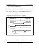
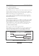
Table 23.5 SDRAMφ Pin State in Each Processing State
Register Setting
SDPSTP DDR
Normal
Operating State
Sleep Mode
Software
Standby Mode
Hardware
Standby Mode
All Module
Clocks Stop
Mode
0 X SDRAMφ output SDRAMφ output Fixed low High impedance SDRAMφ
output
1 0 High impedance High impedance High impedance High impedance High
impedance
1 1 PH1/CS5/RAS5
output
H1/CS5/RAS5
output
H1/CS5/RAS5
output
High impedance H1/CS5/RAS5
output
Note: SDRAM is not available in the H8S/2426 and H8S/2424 Groups.
In these products, this pin functions as a general pin regardless of the SDPSTP bit setting.