
Datasheet


Section 23 Power-Down Modes
R01UH0310EJ0500 Rev. 5.00 Page 1159 of 1384
Sep 25, 2012
H8S/2426, H8S/2426R, H8S/2424 Group
23.3 φ Clock Output Control
Output of the φ clock can be controlled by means of the PSTOP bit in SCKCR, and DDR for the
corresponding port. When the PSTOP bit is set to 1, the φ clock stops at the end of the bus cycle,
and φ output goes high. φ clock output is enabled when the PSTOP bit is cleared to 0. When DDR
for the corresponding port is cleared to 0, φ clock output is disabled and input port mode is set.
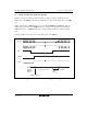
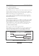
Table 23.4 shows the state of the φ pin in each processing state.
Table 23.4 φ Pin State in Each Processing State
Register Setting
DDR PSTOP
Normal
Operating State
Sleep Mode
Software
Standby Mode
Hardware
Standby Mode
All Module
Clocks Stop
Mode
0 X High impedance High impedance High impedance High impedance High
impedance
1 0 φ output φ output Fixed high High impedance φ output
1 1 Fixed high Fixed high Fixed high High impedance Fixed high