
Datasheet


Section 23 Power-Down Modes
Page 1158 of 1384 R01UH0310EJ0500 Rev. 5.00
Sep 25, 2012
H8S/2426, H8S/2426R, H8S/2424 Group
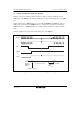
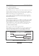
Table 23.3 Combinations of SYSCR Settings and Operation in Access to On-Chip RAM
Register Settings
RAME EXPE mstp Target for Access Description
1 ⎯ This area is not readable/writable and access is
prohibited.
1 X
0 On-chip RAM
1 X External address
space
0
0 X ⎯ This area is not readable/writable and access is
prohibited.
23.2.6 All Module Clocks Stop Mode
When the ACSE bit in MSTPCRH is set to 1 and module stop state is set for all the on-chip
peripheral functions controlled by MSTPCR or EXMSTPCR (MSTPCR = H'FFFF, EXMSTPCR
= H'FFFF), or for all the on-chip peripheral functions except the 8-bit timer (MSTPCR = H'FFFE,
EXMSTPCR = H'FFFF), executing a SLEEP instruction while the SSBY bit in SBYCR is cleared
to 0 will cause all the on-chip peripheral functions (except the 8-bit timer and watchdog timer), the
bus controller, and the I/O ports to stop operating, and a transition to be made to all module clocks
stop mode at the end of the bus cycle.
Operation or stopping of the 8-bit timer can be selected by means of the MSTP0 bit.
To further reduce the current consumption in all module clocks stop mode, stop the modules
controlled by RMMSTPCR (RMMSTPCR = H'FFFF).
All module clocks stop mode is cleared by an external interrupt (NMI, IRQ0 to IRQ15* pins),
RES pin input, or an internal interrupt (8-bit timer, watchdog timer), and the CPU returns to the
normal program execution state via the exception handling state. All module clocks stop mode is
not cleared if interrupts are disabled, if interrupts other than NMI are masked by the CPU, or if the
relevant interrupt is designated as a DTC activation source.
When the STBY pin is driven low, a transition is made to hardware standby mode.
Note: * IRQ8 to IRQ15 are not supported by the H8S/2424 group.