
Datasheet


Section 3 MCU Operating Modes
Page 88 of 1384 R01UH0310EJ0500 Rev. 5.00
Sep 25, 2012
H8S/2426, H8S/2426R, H8S/2424 Group
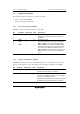
3.3.6 Pin Functions
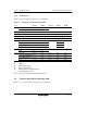
Table 3.2 shows the pin functions in each operating mode.
Table 3.2 Pin Functions in Each Operating Mode
Port Mode 1 Mode 2 Mode 3 Mode 4 Mode 7
Port A PA7 to PA5 P*/A P*/A P*/A P*/A P*/A
PA4 to PA0 A A
Port B A A P*/A P*/A P*/A
Port C A A P*/A P*/A P*/A
Port D D D P*/D D P*/D
Port E P/D* P*/D P*/D P*/D P*/D
Port F PF7, PF6 P/C* P/C* P*/C P/C* P*/C
PF5, PF4 C C C
PF3 P/C* P/C* P/C*
PF2 to PF0 P*/C P*/C P*/C
Port G PG6 to PG1 P*/C P*/C P*/C P*/C P*/C
PG0 P/C* P/C*
Port H PH3, PH2 P*/C P*/C P*/C P*/C P*/C
PH1 (H8S/2426R Group) P/C* P/C* P/C* P/C* P/C*
PH1 (H8S/2426 Group) P*/C P*/C P*/C P*/C P*/C
PH0 P*/C P*/C P*/C P*/C P*/C
[Legend]
P: I/O port
A: Address bus output
D: Data bus input/output
C: Control signals, clock input/output
*: Immediately after a reset
Note: Port H is not supported in the H8S/2424 Group.
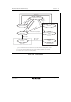
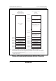
3.4 Memory Map in Each Operating Mode
Figures 3.1 to 3.5 show memory maps in each operating mode.