
Datasheet


Section 23 Power-Down Modes
R01UH0310EJ0500 Rev. 5.00 Page 1149 of 1384
Sep 25, 2012
H8S/2426, H8S/2426R, H8S/2424 Group
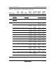
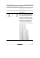
• EXMSTPCRL
Bit Bit Name Initial Value R/W Module
7 MSTP23 1 R/W Synchronous serial communication unit (SSU)
6 MSTP22 1 R/W I
2
C bus interface 2_3 (IIC2_3)
5 MSTP21 1 R/W I
2
C bus interface 2_2 (IIC2_2)
4 MSTP20 1 R/W I
2
C bus interface 2_1 (IIC2_1)
3 MSTP19 1 R/W I
2
C bus interface 2_0 (IIC2_0)
2 MSTP18 1 R/W Reserved
This bit can be read or written to. The write value
should always be 1.
1 MSTP17 1 R/W Reserved
This bit can be read or written to. The write value
should always be 1.
0 MSTP16 1 R/W ⎯
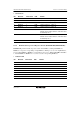
23.1.4 RAM Module Stop Control Registers H and L (RMMSTPCRH, RMMSTPCRL)
RMMSTPCR performs module stop state control of the RAM area. Setting bits MSTP32 to
MSTP39 to 1 stops the corresponding on-chip RAM area. During access to an on-chip RAM area,
do not set bits MSTP32 to MSTP39 corresponding to the area to 1. While bit RAME in SYSCR is
1, and bits MSTP32 to MSTP39 are 1, do not access the corresponding RAM area.
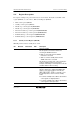
• RMMSTPCRH
Bit Bit Name Initial Value R/W Module
15 MSTP47 0 R/W ⎯
14 MSTP46 0 R/W ⎯
13 MSTP45 0 R/W ⎯
12 MSTP44 0 R/W ⎯
11 MSTP43 0 R/W ⎯
10 MSTP42 0 R/W ⎯
9 MSTP41 0 R/W ⎯
8 MSTP40 0 R/W ⎯