
Datasheet


Section 22 Clock Pulse Generator
Page 1138 of 1384 R01UH0310EJ0500 Rev. 5.00
Sep 25, 2012
H8S/2426, H8S/2426R, H8S/2424 Group
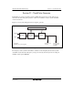
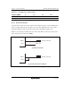
22.3 System-Clock PLL Circuit and Divider
The system-clock PLL circuit and divider have the function of multiplying the frequency of the
clock from the oscillator by a factor of 1, 2, or dividing by 2. The system clock frequency is set
with the STC1 and STC0 bits in PLLCR. The phase of the rising edge of the internal clock is
controlled so as to match that of the rising edge of the EXTAL pin.
When the frequency is changed with the system-clock PLL circuit and divider, operation varies
according to the setting of the STCS bit in SCKCR.
When STCS = 0, the setting of the changed frequency becomes valid after a transition to software
standby mode. The transition time count is performed in accordance with the setting of bits STS3
to STS0 in SBYCR. For details on SBYCR, see section 23.1.1, Standby Control Register
(SBYCR).
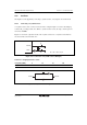
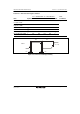
1. The initial PLL circuit multiplication factor is 1.
2. A value is set in bits STS3 to STS0 to give the specified transition time.
3. The target value is set in bits STC1 and STC0, and a transition is made to software standby
mode.
4. The clock pulse generator stops and the value set in STC1 and STC0 becomes valid.
5. Software standby mode is cleared, and a transition time is secured in accordance with the
setting in STS3 to STS0.
6. After the set transition time has elapsed, this LSI resumes operation using the target
multiplication factor.
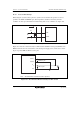
When STCS = 1, a change to the frequency setting becomes effective a maximum of four cycles
after the setting is changed. If the clock frequency is changed during access to an external address
space, correct operation cannot be guaranteed. Therefore, be sure to store instructions that change
the STC1 and STC0 bits and other instructions to be executed within a maximum of four cycles
after the change to the frequency setting in on-chip ROM or on-chip RAM, so that instructions do
not access an external address space before the frequency clock is switched over.