
Datasheet


Section 21 Flash Memory
Page 1094 of 1384 R01UH0310EJ0500 Rev. 5.00
Sep 25, 2012
H8S/2426, H8S/2426R, H8S/2424 Group
21.5 Status Register
The status register indicates the state of flash memory operation and whether erasure or
programming has ended successfully or with an error. The status register contents can be read
through the FMRDY, FMPRSF, and FMERSF bits in FLMSTR.
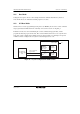
Table 21.6 shows the status register.
In the EW0 mode, the status register can be read with the following timing.
• When a read status register command is issued and then an even address in the user ROM or
data flash is read
• When a program command, a block erase command, or a block blank check command is
issued and then an even address in the user ROM or data flash is read before a read array
command is issued
Table 21.6 Status Register
Status
Bits in Status
Register
Bits in
FMLSTR
Status Name 0 1
Value after
Reset
SR0 (D0) ⎯ Reserved ⎯ ⎯ ⎯
SR1 (D1) ⎯ Reserved ⎯ ⎯ ⎯
SR2 (D2) ⎯ Reserved ⎯ ⎯ ⎯
SR3 (D3) ⎯ Reserved ⎯ ⎯ ⎯
SR4 (D4) FMPRSF Programming
status
Completed
successfully
Ended with
error
0
SR5 (D5) FMERSF Erase status Completed
successfully
Ended with
error
0
SR6 (D6) ⎯ Reserved ⎯ ⎯
SR7 (D7) FMRDY Sequencer status Busy Ready 1
[Legend]
SR0 to SR7: Status register data
D0 to D7: Data bus from which the bit is read when a read status register command is issued.
Note: The FMERSF (SR5) and FMPRSF (SR4) bits are cleared to 0 by a clear status register
command.
When the FMERSF (SR5) or FMPRSF (SR4) bit is 1, the program, block erase, and block
blank check commands are not accepted.