
Datasheet


Section 21 Flash Memory
R01UH0310EJ0500 Rev. 5.00 Page 1087 of 1384
Sep 25, 2012
H8S/2426, H8S/2426R, H8S/2424 Group
21.4 Software Commands
The following describes the software commands. A command or data should be read or written in
16-bit units at an even address in the user ROM or data flash area. When a command code is
written, the lower eight bits (D7 to D0) are ignored.
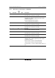
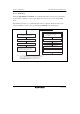
Table 21.5 List of Software Commands
First Bus Cycle Second Bus Cycle Third Bus Cycle
Software
Command Mode Address
Data
(D15 to
D0)
Mode Address
Data
(D15 to
D0)
Mode Address
Data
(D15 to
D0)
Read array Write x H'FFxx
Read status
register
Write x H'70xx Read x SRD
Clear status
register
Write x H'50xx
Program Write WA0 H'41xx Write WA0 WD0 Write WA1 WD1
Block erase Write x H'20xx Write BA H'D0xx
Block blank
check
Write x H'25xx Write BA H'D0xx
[Legend]
SRD: Status register data (D7 to D0)
WA0: Address to write the lower word (the address for the first bus cycle must be the same even
address as that for the second bus cycle).
WA1: Address to write the upper word
WD0: Lower word of write data (16 bits)
WD1: Upper word of write data (16 bits)
BA: Lowest address of the block (note that this should be an even address).
(i.e. H'0000 0000 for block 0, H'0001 0000 for block 1)
x: A desired even address in the user ROM, data flash, or user boot ROM.
xx: Lower eight bits of command code (ignored)