
Datasheet


Section 19 Synchronous Serial Communication Unit (SSU)
Page 1066 of 1384 R01UH0310EJ0500 Rev. 5.00
Sep 25, 2012
H8S/2426, H8S/2426R, H8S/2424 Group
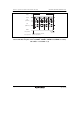
19.4.6 SCS Pin Control and Conflict Error
When bits CSS1 and CSS0 in SSCRH are specified to B'10 and the SSUMS bit in SSCRL is
cleared to 0, the SCS pin functions as an input (Hi-Z) to detect conflict error. The conflict
detection period is from setting the MSS bit in SSCRH to 1 to starting serial transfer and after
transfer ends. When a low level signal is input to the SCS pin within the period, a conflict error
occurs. At this time, the CE bit in SSSR is set to 1 and the MSS bit is cleared to 0.
Note: While the CE bit is set to 1, transmission or reception is not resumed. Clear the CE bit to 0
before resuming the transmission or reception.
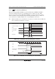
CE
Data written
to SSTDR
Maximum time for
internally clocking SCS
MSS
Internal signal for
transfer enable
SCS output
External input to SCS
Internal-clocked SCS
(Hi-Z)
Conflict error
detection period
Figure 19.10 Conflict Error Detection Timing (Before Transfer)
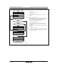
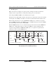
φ
SCS
MSS
CE
(Hi-Z)
Transfer
end
Internal signal for
transfer enable
Conflict error detection period
Figure 19.11 Conflict Error Detection Timing (After Transfer End)