
Datasheet


Section 19 Synchronous Serial Communication Unit (SSU)
R01UH0310EJ0500 Rev. 5.00 Page 1051 of 1384
Sep 25, 2012
H8S/2426, H8S/2426R, H8S/2424 Group
19.4 Operation
19.4.1 Transfer Clock
A transfer clock can be selected from eight internal clocks and an external clock. When using this
module, set the SCKS bit in SSCRH to 1 to select the SSCK pin as a serial clock. When the MSS
bit in SSCRH is 1, an internal clock is selected and the SSCK pin is used as an output pin. When
transfer is started, the clock with the transfer rate set by bits CKS2 to CKS0 in SSMR is output
from the SSCK pin. When MSS = 0, an external clock is selected and the SSCK pin is used as an
input pin.
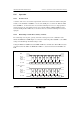
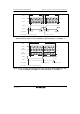
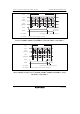
19.4.2 Relationship of Clock Phase, Polarity, and Data
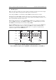
The relationship of clock phase, polarity, and transfer data depends on the combination of the
CPOS and CPHS bits in SSMR. Figure 19.2 shows the relationship. When SSUMS = 1, the CPHS
setting is invalid although the CPOS setting is valid.
Setting the MLS bit in SSMR selects that MSB or LSB first communication. When MLS = 0, data
is transferred from the LSB to the MSB. When MLS = 1, data is transferred from the MSB to the
LSB.
SSCK
(CPOS = 0)
(1) When CPHS = 0
(2) When CPHS = 1
SSCK
(CPOS = 1)
SSI, SSO
SCS
Bit 0 Bit 1 Bit 2 Bit 3 Bit 4 Bit 5 Bit 6 Bit 7
SSCK
(CPOS = 0)
SSCK
(CPOS = 1)
SSI, SSO
SCS
Bit 0 Bit 1 Bit 2 Bit 3 Bit 4 Bit 5 Bit 6 Bit 7
Figure 19.2 Relationship of Clock Phase, Polarity, and Data