
Datasheet

Section 19 Synchronous Serial Communication Unit (SSU)
Page 1048 of 1384 R01UH0310EJ0500 Rev. 5.00
Sep 25, 2012
H8S/2426, H8S/2426R, H8S/2424 Group
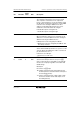
Bit Bit Name
Initial
Value R/W Description
3 SCSATS 0 R/W Selects the assertion timing of the SCS pin (valid in
SSU and master mode).
0: Min. values of t
LEAD
and t
LAG
are 1/2 × t
SUcyc
1: Min. values of t
LEAD
and t
LAG
are 3/2 × t
SUcyc
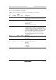
2 SSODTS 0 R/W Selects the data output timing of the SSO pin (valid in
SSU and master mode)
0: While BIDE = 0, MSS = 1, and TE = 1 or while BIDE
= 1, TE = 1, and RE = 0, the SSO pin outputs data
1: While BIDE = 0, MSS = 1, and TE = 1 or while BIDE
= 1, TE = 1, and RE = 0, the SSO pin outputs data
while the SCS pin is driven low
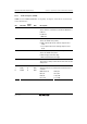
1, 0 ⎯ All 0 R/W Reserved
These bits are always read as 0. The write value should
always be 0.