
Datasheet


Section 19 Synchronous Serial Communication Unit (SSU)
R01UH0310EJ0500 Rev. 5.00 Page 1039 of 1384
Sep 25, 2012
H8S/2426, H8S/2426R, H8S/2424 Group
19.2 Input/Output Pins
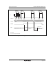
Table 19.1 shows the SSU pin configuration.
Table 19.1 Pin Configuration
Channel Symbol I/O Function
0 SSCK0 I/O SSU clock input/output
SSI0 I/O SSU data input/output
SSO0 I/O SSU data input/output
SCS0 I/O SSU chip select input/output
Note: * Because channel numbers are omitted in later descriptions, these are shown SSCK,
SSI, SSO, and SCS.
19.3 Register Descriptions
The SSU has the following registers.
• SS control register H_0 (SSCRH_0)
• SS control register L_0 (SSCRL_0)
• SS mode register_0 (SSMR_0)
• SS enable register_0 (SSER_0)
• SS status register_0 (SSSR_0)
• SS control register 2_0 (SSCR2_0)
• SS transmit data register 0_0 (SSTDR0_0)
• SS transmit data register 1_0 (SSTDR1_0)
• SS transmit data register 2_0 (SSTDR2_0)
• SS transmit data register 3_0 (SSTDR3_0)
• SS receive data register 0_0 (SSRDR0_0)
• SS receive data register 1_0 (SSRDR1_0)
• SS receive data register 2_0 (SSRDR2_0)
• SS receive data register 3_0 (SSRDR3_0)
• SS shift register_0 (SSTRSR_0)