
Datasheet


Section 17 A/D Converter
R01UH0310EJ0500 Rev. 5.00 Page 1023 of 1384
Sep 25, 2012
H8S/2426, H8S/2426R, H8S/2424 Group
17.7.7 Notes on Board Design
In board design, digital circuitry and analog circuitry should be as mutually isolated as possible,
and layout in which digital circuit signal lines and analog circuit signal lines cross or are in close
proximity should be avoided as far as possible. Failure to do so may result in incorrect operation
of the analog circuitry due to inductance, adversely affecting A/D conversion values.
Digital circuitry must be isolated from the analog input pins (AN0 to AN15*), analog reference
power supply (Vref), and analog power supply (AVcc) by the analog ground (AVss). Also, the
analog ground (AVss) should be connected at one point to a stable ground (Vss) on the board.
Note: * In the H8S/2424 group, only AN0 to AN7, AN11, and AN12 are available as analog
input pins.
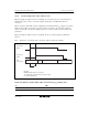
17.7.8 Notes on Noise Countermeasures
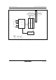
A protection circuit connected to prevent damage due to an abnormal voltage such as an excessive
surge at the analog input pins (AN0 to AN15*) should be connected between AVcc and AVss as
shown in figure 17.12. Also, the bypass capacitors connected to AVcc and the filter capacitor
connected to the AN0 to AN11 pins must be connected to AVss.
If a filter capacitor is connected, the input currents at the AN0 to AN15* pins are averaged, and so
an error may arise. Also, when A/D conversion is performed frequently, as in scan mode, if the
current charged and discharged by the capacitance of the sample-and-hold circuit in the A/D
converter exceeds the current input via the input impedance (R
in
), an error will arise in the analog
input pin voltage. Careful consideration is therefore required when deciding the circuit constants.
Note: * In the H8S/2424 group, only AN0 to AN7, AN11, and AN12 are available as analog
input pins.