
Datasheet


Section 17 A/D Converter
R01UH0310EJ0500 Rev. 5.00 Page 1021 of 1384
Sep 25, 2012
H8S/2426, H8S/2426R, H8S/2424 Group
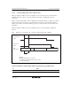
17.7.4 Permissible Signal Source Impedance
This LSI's analog input is designed so that the conversion accuracy is guaranteed for an input
signal for which the signal source impedance is 5 kΩ or less. This specification is provided to
enable the A/D converter's sample-and-hold circuit input capacitance to be charged within the
sampling time; if the sensor output impedance exceeds 5 kΩ, charging may be insufficient and it
may not be possible to guarantee the A/D conversion accuracy. However, if a large capacitance is
provided externally for conversion in single mode, the input load will essentially comprise only
the internal input resistance of 5 kΩ, and the signal source impedance is ignored. However, since a
low-pass filter effect is obtained in this case, it may not be possible to follow an analog signal with
a large differential coefficient (e.g., 5 mV/μs or greater) (see figure 17.11). When converting a
high-speed analog signal or conversion in scan mode, a low-impedance buffer should be inserted.
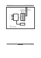
Equivalent circuit of the A/D converter
This LSI
7 pF
Cin =
15 pF
10 kΩ
Low-pass
filter
C to 0.1 μF
Sensor output
impedance
R to 5 kΩ
Sensor input
Figure 17.11 Example of Analog Input Circuit