
Datasheet

Section 17 A/D Converter
R01UH0310EJ0500 Rev. 5.00 Page 999 of 1384
Sep 25, 2012
H8S/2426, H8S/2426R, H8S/2424 Group
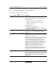
17.3.2 A/D Control/Status Register for Unit 0 (ADCSR_0)
ADCSR_0 controls A/D conversion operations.
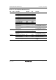
Bit Bit Name
Initial
Value R/W Description
7 ADF 0 R/(W)* A/D End Flag
A status flag that indicates the end of A/D conversion.
[Setting conditions]
• Completion of A/D conversion in single mode
• Completion of A/D conversion on all specified
channels in scan mode
[Clearing conditions]
• Writing of 0 after reading ADF = 1
• Reading from ADDR after activation of the DMAC or
DTC by an ADI interrupt
6 ADIE 0 R/W
A/D Interrupt Enable
Setting this bit to 1 enables ADI interrupts by ADF.
5 ADST 0 R/W
A/D Start
Clearing this bit to 0 stops A/D conversion, and the A/D
converter enters wait state.
Setting this bit to 1 starts A/D conversion. In single mode,
this bit is cleared to 0 automatically when A/D conversion
on the specified channel ends. In scan mode, A/D
conversion continues sequentially on the specified
channels until this bit is cleared to 0 by software, a reset,
or hardware standby mode. While the ADSTCLR bit in
ADCR is set to 1, the ADST bit is cleared to 0
automatically when A/D conversion on all selected
channels ends, and then A/D conversion stops.
The timing to clear the ADST bit automatically differs
from that of ADF setting; the ADST bit is cleared before
the ADF bit is set.
4 EXCKS 0 R/W
Clock Extension Select
Specifies the A/D conversion time in combination with the
CKS1 and CKS0 bits in ADCR. Be sure to set these three
bits at one time. For details, see the description of the
ADCR resisters.