
Datasheet

Section 16 I2C Bus Interface 2 (IIC2)
R01UH0310EJ0500 Rev. 5.00 Page 981 of 1384
Sep 25, 2012
H8S/2426, H8S/2426R, H8S/2424 Group
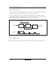
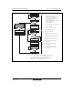
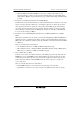
16.4.6 Noise Canceler
The logic levels at the SCL and SDA pins are routed through noise cancelers before being latched
internally. Figure 16.13 shows a block diagram of the noise canceler circuit.
The noise canceler consists of two cascaded latches and a match detector. The SCL (or SDA)
input signal is sampled on the system clock, but is not passed forward to the next circuit unless the
outputs of both latches agree. If they do not agree, the previous value is held.
C
QD
March detector
Internal
SCL or SDA
signal
SCL or SDA
input signal
Sampling
clock
Sampling clock
System clock
period
Latch
Latch
C
Q
D
Figure 16.13 Block Diagram of Noise Canceler
16.4.7 Example of Use
Flowcharts in respective modes that use the I
2
C bus interface are shown in figures 16.14 to 16.17.