
Datasheet


Section 22 Clock Pulse Generator
Page 1140 of 1384 R01UH0310EJ0500 Rev. 5.00
Sep 25, 2012
H8S/2426, H8S/2426R, H8S/2424 Group
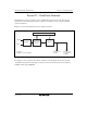
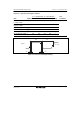
22.4.3 Notes on Board Design
When using the crystal resonator, place the crystal resonator and its load capacitors as close as
possible to the XTAL and EXTAL pins. Other signal lines should be routed away from the
oscillation circuit to prevent induction from interfering with correct oscillation. See figure 22.6.
C
L2
Signal A Signal B
C
L1
This LSI
XTAL
EXTAL
Prohibited
Figure 22.6 Note on Board Design for Oscillation Circuit
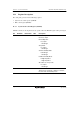
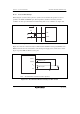
Figure 22.7 shows the external circuitry recommended for the PLL circuit. Separate PLLVcc and
PLLVss from the other Vcc and Vss lines at the board power supply source, and be sure to insert
bypass capacitors CPB and CB close to the pins.
PLLV
CC
PLLV
SS
V
CC
V
SS
CPB: 0.1 µF
*
CB: 0.1 µF
*
Note: * CB and CPB are laminated ceramic capacitors.
Figure 22.7 Recommended External Circuitry for PLL Circuit