38C1 Group REJ03B0075-0240Z Rev.2.40 2004.6.14 SINGLE-CHIP 8-BIT CMOS MICROCOMPUTER • LCD drive control circuit DESCRIPTION The 38C1 group is the 8-bit microcomputer based on the 740 family core technology. The 38C1 group has the LCD drive control circuit, an 8-channel A/ D converter, and serial I/O as additional functions. The various microcomputers in the 38C1 group include variations of internal memory size and packaging. For details, refer to the section on part numbering.
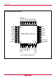
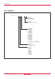
38C1 Group P03/SEG3 P04/SEG4 P05/SEG5 P06/SEG6 P07/SEG7 SEG8 SEG9 SEG10 SEG11 SEG12 SEG13 SEG14 SEG15 SEG16 COM3 COM2 PIN CONFIGURATION (TOP VIEW) 48 47 46 45 44 43 42 41 40 39 38 37 36 35 34 33 P02/SEG2 P01/SEG1 P00/SEG0 P57/SRDY P56/SCLK P55/SOUT P54/SIN P53/CNTR1 P52/CNTR0 P51/INT1 P50/INT0 P47/AN7 P46/AN6 P45/AN5 P44/AN4 AN3/ADKEY3 49 32 50 31 51 30 52 29 53 28 54 27 55 26 M38C1XMX-XXXFP/HP 56 57 23 59 22 60 21 61 20 62 19 63 18 64 17 3 4 5 6 7 8 9 10 11 12 13
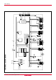
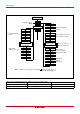
page 3 of 56 φ On-chip oscillator 5 6 XCOUT Subclock output 9 10 P6(5) XCIN Subclock input I/O port P6 4 13 12 XCIN XCOUT φ Clock generating circuit Main clock output XOUT Main clock input XIN TOUT Jun 14, 2004 1 64 Analog input AN 3 2 A/D converter (8) PCH CPU I/O port P5 52 53 54 55 56 57 58 59 SI/O(8) Timer 3 (8) Timer Y (16) Timer 1 (8) Timer 2 (8) Timer X (16) ROM 63 62 61 60 Data bus 11 (0 V) VSS P5(8) 14 (5 V) VCC P4(4) I/O port P4 PS PCL S Y X A 8 Res
38C1 Group PIN DESCRIPTION Table 1 Pin description Pin Function Name VCC, VSS Power source • Apply voltage of power source to VCC, and 0 V to VSS. CNVSS CNVSS • Connect to Vss. RESET Reset input Clock input • Reset input pin for active “L”. • Input and output pins for the main clock generating circuit.
38C1 Group PART NUMBERING Product M38C1 3 M 6 - XXX FP Package type FP : 64P6U-A package HP : 64P6Q-A package ROM number Omitted in One Time PROM version. ROM/PROM size 1 : 4096 bytes 2 : 8192 bytes 3 : 12288 bytes 4 : 16384 bytes 5 : 20480 bytes 6 : 24576 bytes 7 : 28672 bytes 8 : 32768 bytes 9 : 36864 bytes A : 40960 bytes B : 45056 bytes C : 49152 bytes D : 53248 bytes E : 57344 bytes F : 61440 bytes The first 128 bytes and the last 2 bytes of ROM are reserved areas ; they cannot be used.
38C1 Group GROUP EXPANSION Packages Renesas plans to expand the 38C1 group as follows. 64P6Q-A .................................... 0.5 mm-pitch plastic molded QFP 64P6U-A .................................... 0.8 mm-pitch plastic molded QFP Memory Type Support for Mask ROM version, One Time PROM version. Memory Size ROM/PROM size ............................................... 16 K to 24 K bytes RAM size ..............................................................
38C1 Group FUNCTIONAL DESCRIPTION CENTRAL PROCESSING UNIT (CPU) [Stack Pointer (S)] The stack pointer is an 8-bit register used during subroutine calls and interrupts. This register indicates start address of stored area (stack) for storing registers during subroutine calls and interrupts. The low-order 8 bits of the stack address are determined by the contents of the stack pointer. The high-order 8 bits of the stack address are determined by the stack page selection bit.
38C1 Group On-going Routine Interrupt request (Note) M (S) Execute JSR Push return address on stack M (S) (PCH) (S) (S) – 1 M (S) (PCL) (S) (S)– 1 (S) M (S) (S) M (S) (S) Subroutine POP return address from stack (S) + 1 (PCL) M (S) (S) (S) + 1 (PCH) M (S) (S) – 1 (PCL) Push return address on stack (S) – 1 (PS) Push contents of processor status register on stack (S) – 1 Interrupt Service Routine Execute RTS (S) (PCH) I Flag is set from “0” to “1” Fetch the jump vector Execute
38C1 Group [Processor status register (PS)] The processor status register is an 8-bit register consisting of 5 flags which indicate the status of the processor after an arithmetic operation and 3 flags which decide MCU operation. Branch operations can be performed by testing the Carry (C) flag , Zero (Z) flag, Overflow (V) flag, or the Negative (N) flag. In decimal mode, the Z, V, N flags are not valid.
38C1 Group [CPU Mode Register (CPUM)] 003B16 The CPU mode register contains the stack page selection bit and the internal system clock selection bit. The CPU mode register is allocated at address 003B16. After system is released from reset, the on-chip oscillator mode is selected, and the XIN–XOUT oscillation and the XCIN–XCOUT oscillation are stopped.
38C1 Group MEMORY Special Function Register (SFR) Area The Special Function Register area in the zero page contains control registers such as I/O ports and timers. RAM RAM is used for data storage and for stack area of subroutine calls and interrupts. Zero Page The 256 bytes from addresses 0000 16 to 00FF 16 are called the zero page area. The internal RAM and the special function registers (SFR) are allocated to this area.
38C1 Group 000016 Port P0 (P0) 002916 Timer X (low) (TXL) Timer X (high) (TXH) Timer Y (low) (TYL) Timer Y (high) (TYH) Timer 1 (T1) Timer 2 (T2) Timer 3 (T3) Timer X mode register (TXM) Timer Y mode register (TYM) Timer 123 mode register (T123M) 002A16 φ output control register 002016 000116 002116 000216 002216 000316 002316 000416 000516 000616 000716 000816 000916 000A16 000B16 000C16 000D16 Port P2 (P2) Port P2 direction register (P2D) Port P3 (P3) Port P3 direction register (P3D) Port P
38C1 Group I/O PORTS Direction Registers (Ports P2–P6) Pull-up/Pull-down Control The I/O ports (P2–P6) have direction registers which determine the input/output direction of each individual pin. When “0” is written to the bit corresponding to a pin, that pin becomes an input pin. When “1” is written to that bit, that pin becomes an output pin. If data is read from a pin set to output, the value of the port output latch is read, not the value of the pin itself. Pins set to input are floating.
38C1 Group Table 5 List of I/O port function Name Pin Input/Output COM0–COM3 Common P00/SEG0– Input Port P0 Input, P07/SEG7 SEG8–/SEG16 Segment Output I/O Format Non-Port Function LCD common output CMOS compatible Related SFRs LCD mode register LCD segment output PULL register individual bits input level Segment output enable register LCD0–LCD3 Output LCD mode register LCD segment output Fig. No.
38C1 Group (1)Port P0 (2)Port P2 VL2/VL3 VL2/VL3 VL1/VSS Segment output enable bit VL1/VSS Direction register Data bus Data bus Segment output enable bit Port latch Pull-down control Segment output enable bit Pull-down control (3)Port P30–P34, P50, P51 (4)Port P4 Pull-up control Pull-up control Direction register Direction register Data bus Data bus Port latch Analog input pin selection bit Key input (key-on wakeup) interrupt input INT0, INT1 interrupt input (5)Port P52 Port latch A/
38C1 Group (7)Port P54 (8)Port P55 Pull-up control Direction register Data bus P55/SOUT P-channel output disable bit Data bus Port latch (9)Port P56 Port latch Serial I/O output Serial I/O input (10)Port P57 Pull-up control Pull-up control Synchronous clock selection bit Serial I/O port selection bit SRDY output selection bit Direction register Serial I/O port selection bit Direction register Data bus Pull-up control Serial I/O transmit end signal Synchronous clock selection bit Serial I/O
38C1 Group (14)Port P63 (13)Port P62 Pull-up control Pull-up control Direction register Port latch Data bus Direction register Data bus Port latch φ output control bit φ TOUT output control bit Timer output (15)AN0/ADKEY0–AN3/ADKEY3 ADKEY selection bit (16)COM0–COM3 VL3 ADKEY enable bit Analog input selection bit A/D conversion input VL2 VL1 The gate input signal of each transistor is controlled by the LCD duty ratio and the bias value.
38C1 Group INTERRUPTS Interrupt Operation Interrupts occur by thirteen sources: five external, seven internal, and one software. By acceptance of an interrupt, the following operations are automatically performed: 1. The contents of the program counter and the processor status register are automatically pushed onto the stack. 2. The interrupt disable flag is set and the corresponding interrupt request bit is cleared. 3.
38C1 Group Interrupt request bit Interrupt enable bit Interrupt disable flag (I) Interrupt request BRK instruction Reset Fig.
38C1 Group Key Input Interrupt (Key-on Wake Up) A Key-on wake up interrupt request is generated by applying “L” level voltage to any pin of port P3 that have been set to input mode. In other words, it is generated when AND of input level goes from “1” to “0”. An example of using a key input interrupt is shown in Figure 17, where an interrupt request is generated by pressing one of the keys consisted as an active-low key matrix which inputs to ports P30–P33.
38C1 Group TIMERS Read and write operation on 16-bit timer must be performed for both high- and low-order bytes. When reading a 16-bit timer, read the high-order byte first. When writing to a 16-bit timer, write the low-order byte first. The 16-bit timer cannot perform the correct operation when reading during the write operation, or when writing during the read operation. The 38C1 group has five timers: timer X, timer Y, timer 1, timer 2, and timer 3.
38C1 Group Timer X Timer X is a 16-bit timer that can be selected in one of four modes and can be controlled the timer X write and the real time port by setting the timer X mode register.
38C1 Group Timer Y b7 Timer Y is a 16-bit timer that can be selected in one of four modes. (1) Timer mode The timer counts the followings; • f(XIN)/16 in middle-, or high-speed mode • f(XCIN)/16 in low-speed mode • f(XROSC) divided by 16 in on-chip oscillator mode (2) Period measurement mode CNTR 1 interrupt request is generated at rising/falling edge of CNTR1 pin input signal. Simultaneously, the value in timer Y latch is reloaded in timer Y and timer Y continues counting down.
38C1 Group Timer 1, Timer 2, Timer 3 Timer 1, timer 2, and timer 3 are 8-bit timers. The count source for each timer can be selected by timer 123 mode register. The timer latch value is not affected by a change of the count source. However, because changing the count source may cause an inadvertent count down of the timer. Therefore, rewrite the value of timer whenever the count source is changed.
38C1 Group Serial I/O b7 b0 The serial I/O function can be used only for clock synchronous serial I/O. For clock synchronous serial I/O, the transmitter and the receiver must use the same clock. When the internal clock is used, transfer is started by a write signal to the serial I/O register.
38C1 Group Transfer clock (Note 1) Serial I/O register write signal (Note 2) Serial I/O output SOUT D0 D1 D2 D3 D4 D5 D6 D7 Serial I/O input SIN Serial I/O interrupt request bit set Notes 1: When the internal clock is selected as the transfer clock, the divide ratio can be selected by setting bits 0 to 2 of the serial I/O control register. 2: When the internal clock is selected as the transfer clock, the SOUT pin goes to high impedance after transfer completion.
38C1 Group A/D CONVERTER Comparator and Control Circuit The functional blocks of the A/D converter are described below. The comparator and control circuit compare an analog input voltage with the comparison voltage and store the result in the A/D conversion register. When an A/D conversion is completed, the control circuit sets the AD conversion completion bit and the AD interrupt request bit to “1”. The comparator is constructed linked to a capacitor.
38C1 Group ADKEY Control Circuit The ADKEY function is the function for A/D conversion of the “L” level analog input voltage input to the ADKEY pin automatically. This function can be used also in the state of STP and WIT. • ADKEY Selection Two or more ADKEY pins can be selected by the low-order 4 bits of P4 data register. If “L” level input to an ADKEY pin is detected, other bits are set to “0” and only the corresponding ADKEY selection bit is set to “1”.
38C1 Group Definition of A/D converter accuracy The A/D conversion accuracy is defined below (refer to Figure 28). • Relative accuracy ➀ Zero transition voltage (V0T) This means an analog input voltage when the actual A/D conversion output data changes from “0” to “1.” ➁ Full-scale transition voltage (VFST) This means an analog input voltage when the actual A/D conversion output data changes from “255” to ”254.
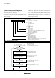
38C1 Group LCD DRIVE CONTROL CIRCUIT The 38C1 group has the built-in Liquid Crystal Display (LCD) drive control circuit consisting of the following. LCD display register Segment output enable register LCD mode register Selector Timing controller Common driver Segment driver Bias control circuit A maximum of 25 segment output pins and 4 common output pins can be used. Up to 100 pixels can be controlled for LCD display.
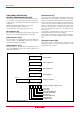
Rev.2.40 Jun 14, 2004 page 31 of 56 P26/SEG23 P27/SEG24 P00/SEG0 P01/SEG1 P02/SEG2 P03/SEG3 SEG16 Segment Segment driver driver Segment Segment Segment Segment driver driver driver driver Fig.
38C1 Group Bias Control and Applied Voltage to LCD Power Input Pins To the LCD power input pins (VL1–VL3), apply the voltage shown in Table 8 according to the bias value. Select a bias value by the bias control bit (bit 2 of the LCD mode register). Common Pin and Duty Ratio Control The common pins (COM 0–COM3) to be used are determined by duty ratio. Select duty ratio by the duty ratio selection bits (bits 0 and 1 of the LCD mode register).
38C1 Group LCD Display register f(LCDCK)= Address 001016 to 001C16 is the LCD display register. When “1” are written to these addresses, the corresponding segments of the LCD display panel are turned on.
38C1 Group Internal logic LCDCK timing 1/4 duty Voltage level VL3 VL2=VL1 VSS COM0 COM1 COM2 COM3 VL3 VSS SEG0 OFF COM3 ON COM2 COM1 OFF COM0 COM3 ON COM2 COM1 COM0 1/3 duty VL3 VL2=VL1 VSS COM0 COM1 COM2 VL3 VSS SEG0 ON OFF COM0 COM2 ON COM1 OFF COM0 COM2 ON COM1 OFF COM0 COM2 1/2 duty VL3 VL2=VL1 VSS COM0 COM1 VL3 VSS SEG0 ON OFF ON OFF ON OFF ON OFF COM1 COM0 COM1 COM0 COM1 COM0 COM1 COM0 1/1 duty (1/1 bias) COM0 VL3 VL2=VL1=VSS SEG0 VL3 VSS OFF
38C1 Group Internal logic LCDCK timing 1/4 duty Voltage level VL3 VL2 VL1 VSS COM0 COM1 COM2 COM3 VL3 SEG0 VSS OFF COM3 ON COM2 COM1 OFF COM0 COM3 ON COM2 COM1 COM0 1/3 duty VL3 VL2 VL1 VSS COM0 COM1 COM2 VL3 SEG0 VSS ON OFF COM0 COM2 ON COM1 OFF COM0 COM2 ON COM1 OFF COM0 COM2 1/2 duty VL3 VL2 VL1 VSS COM0 COM1 VL3 SEG0 VSS ON OFF ON OFF ON OFF ON OFF COM1 COM0 COM1 COM0 COM1 COM0 COM1 COM0 Fig. 34 LCD drive waveform (1/3 bias) Rev.2.
38C1 Group OTHER FUNCTION REGISTERS ● φ clock output function The internal clock φ can be output from port P63 by setting the φ output control register. At φ clock output, set “1” to the bit 3 of the port P6 direction register. b7 b0 φ output control register (CKOUT: address 002A16, initial value: 0016) φ output control bit 0 0 : Port function 0 1 : φ frequency signal output 1 0 : XCIN frequency signal output 1 1 : Not available Not used (returns “0” when read) (Do not write “1” to this bit) Fig.
38C1 Group RESET CIRCUIT Power on To reset the microcomputer, RESET pin should be held at an “L” level for 2 µs or more. Then the RESET pin is returned to an “H” level (the power source voltage should be between VCC(min.) and 5.5 V), reset is released. After the reset is completed, the program starts from the address contained in address FFFD16 (high-order byte) and address FFFC16 (low-order byte). Make sure that the reset input voltage is less than 0.2 VCC for VCC of VCC (min.).
C1 Group Address Register contents (1) Port P2 direction register 000516 0016 (2) Port P3 direction register 000716 0016 (3) Port P4 direction register 000916 0016 (4) Port P5 direction register 000B16 0016 Port P6 direction register 000D16 0016 (6) Serial I/O control register 001D16 0016 (7) Timer X (low) 002016 FF16 (8) Timer X (high) 002116 FF16 (9) Timer Y (low) 002216 FF16 (10) Timer Y (high) 002316 FF16 (11) Timer 1 002416 1016 (12) Timer 2 002516 FF16 (13) Tim
38C1 Group CLOCK GENERATING CIRCUIT The oscillation circuit of 38C1 group can be formed by connecting an oscillator, capacitor and resistor between XIN and XOUT (XCIN and XCOUT). To supply a clock signal externally, input it to the X IN pin and make the XOUT pin open. The clocks that are externally generated cannot be directly input to XCIN. Use the circuit constants in accordance with the oscillator manufacturer's recommended values.
38C1 Group On-chip oscillator XIN XOUT “1” Main clock selection bit CPUM BIT3 “0” XIN-XOUT oscillation stop bit CPUM BIT5 XCOUT XCIN “1” Internal system clock selection bit (Note) “0” CPUM BIT7 “1” Timer 1 count source selection bit T123M BIT 5 “0” “0” Port Xc switch bit CPUM BIT4 1/2 1/4 1/2 Timer 1 “1” Main clock division ratio selection bit “1” CPUM BIT6 Main clock “0” selection bit CPUM BIT3 “0” “1” Internal system clock selection bit “0” CPUM BIT7 “1” Timing φ (Internal clock) Q S
38C1 Group Reset release Low-speed mode On-chip oscillator mode XIN stop XCIN stop φ=f(ROSC)/8 CM7=0 CM6=1 (Note 5) CM5=1 CM4=0 CM3=1 CM4 XIN stop XCIN oscillation φ=f(ROSC)/8 CM7=0 CM6=1 (Note 5) CM5=1 CM4=1 CM3=1 XIN stop XCIN oscillation φ=16kHz CM7=1 CM6=1 CM5=1 CM4=1 CM3=* (Note 9) CM7 CM6 CM4 CM5 CM5 XIN oscillation XCIN stop φ=f(ROSC)/8 CM7=0 CM6=1 (Note 5) CM5=0 CM4=0 CM3=1 CM4 CM5 CM5 XIN oscillation XCIN oscillation φ=f(ROSC)/8 CM7=0 CM6=1(Note 5) CM5=0 CM4=1 CM3=1 CM3 CM3 CM5 XIN
38C1 Group NOTES ON PROGRAMMING Processor Status Register Serial I/O The contents of the processor status register (PS) after a reset are undefined, except for the interrupt disable flag (I) which is “1”. After a reset, initialize flags which affect program execution. In particular, it is essential to initialize the index X mode (T) and the decimal mode (D) flags because of their effect on calculations.
38C1 Group NOTES ON USE VL3 pin Noise When LCD drive control circuit is not used, connect VL3 to VCC. Countermeasures against noise (1) Shortest wiring length ➀ Wiring for RESET pin Make the length of wiring which is connected to the RESET pin as short as possible. Especially, connect a capacitor across the RESET pin and the VSS pin with the shortest possible wiring (within 20mm). ● Reason The width of a pulse input into the RESET pin is determined by the timing necessary conditions.
38C1 Group (3) Oscillator concerns In order to obtain the stabilized operation clock on the user system and its condition, contact the oscillator manufacturer and select the oscillator and oscillation circuit constants. Be careful especially when range of voltage or/and temperature is wide. Also, take care to prevent an oscillator that generates clocks for a microcomputer operation from being affected by other signals.
38C1 Group DATA REQUIRED FOR MASK ORDERS ROM PROGRAMMING METHOD The following are necessary when ordering a mask ROM production: 1.Mask ROM Order Confirmation Form✽ 2.Mark Specification Form✽ 3.Data to be written to ROM, in EPROM form (three identical copies) or one floppy disk The built-in PROM of the blank One Time PROM version (M38C13E6FP/HP) can be read or programmed with a generalpurpose PROM programmer using a special programming adapter. Set the address of PROM programmer in the user ROM area.
38C1 Group ELECTRICAL CHARACTERISTICS Absolute Maximum Ratings Table 11 Absolute maximum ratings Symbol VCC VI VI VI VI VI VI VI VI VO Parameter Power source voltage Input voltage P00–P07, P20–P27, P30–P34, P44–P47, P50–P57, P60–P64 Input voltage VL1 Input voltage VL2 Input voltage VL3 Input voltage RESET, XIN Input voltage AN0–AN3 Input voltage CNVSS (Mask ROM version) Input voltage CNVSS (One Time PROM version) Output voltage P20–P27 VO VO VO Pd Topr Tstg Output voltage P30–P34, P44–P47, P50–P57, P60–
38C1 Group Recommended Operating Conditions Table 12 Recommended operating conditions (Vcc = 1.8 to 5.5 V (One Time PROM version: 2.2 to 5.
38C1 Group Table 13 Recommended operating conditions (Vcc = 1.8 to 5.5 V (One Time PROM version: 2.2 to 5.
38C1 Group Table 14 Recommended operating conditions (Vcc = 1.8 to 5.5 V (One Time PROM version: 2.2 to 5.5 V), Ta = –20 to 85°C, unless otherwise noted) Symbol Parameter f(CNTR0) Timer X and Timer Y f(CNTR1) Input frequency (duty cycle 50%) f(XIN) Main clock input frequency (duty cycle 50%) (Note 1) Condition Limits Min. Typ. (4.0 V ≤ VCC ≤ 5.5 V) (Mask ROM version: 2.0V ≤ VCC ≤ 4.0 V) (One Time PROM version: 3.0 V ≤ VCC ≤ 4.0 V) (Mask ROM version: VCC ≤ 2.0 V) (One Time PROM version: 2.
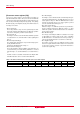
38C1 Group Electrical Characteristics Table 15 Electrical characteristics (Vcc = 4.0 to 5.
38C1 Group Table 16 Electrical characteristics (Vcc = 1.8 to 5.5 V (One Time PROM version: 2.2 to 5.5 V), Ta = –20 to 85°C, f(XCIN) = 32.768 kHz, output transistors “OFF”, AD converter stopped, unless otherwise noted) Limits Symbol Parameter Test conditions Unit Min. Typ. Max. Power High-speed f(XIN) = 8 MHz 3.0 6.0 mA ICC Vcc = 5 V source mode f(XIN) = 8 MHz (in WIT state) 0.8 1.6 mA Mask ROM current f(XIN) = 4 MHz 1.5 3.0 mA version f(XIN) = 8 MHz 4.7 9.4 mA Vcc = 5 V 0.9 1.
38C1 Group A/D Converter Characteristics Table 17 A/D converter recommended operating condition (Vcc = 2.0 to 5.5 V (One Time PROM version: 2.2 to 5.5 V), Ta = –20 to 85°C, unless otherwise noted) Symbol VDD Parameter Power source voltage VIH “H” input voltage ADKEY0–ADKEY3 VIL “L” input voltage ADKEY0–ADKEY3 AD converter control clock (low-speed mode and onchip oscillator mode excluded) f(XIN) Conditions Mask ROM version One Time PROM version Limits Typ. Min. 5.0 2.0 5.0 2.2 0.
38C1 Group Timing Requirements And Switching Characteristics Table 19 Timing requirements 1 (Vcc = 4.0 to 5.
38C1 Group Table 21 Switching characteristics 1 (Vcc = 4.0 to 5.
38C1 Group tC(CNTR) tWL(CNTR) tWH(CNTR) CNTR0,CNTR1 0.8VCC 0.2VCC tWL(INT) tWH(INT) INT0, INT1 0.8VCC 0.2VCC tW(RESET) RESET 0.8VCC 0.2VCC tC(XIN) tWL(XIN) tWH(XIN) 0.8VCC XIN 0.2VCC tC(SCLK) tf SCLK tWL(SCLK) th(SCLK-SIN) 0.8VCC 0.2VCC SIN td(SCLK-SOUT) SOUT Fig. 51 Timing chart Jun 14, 2004 tWH(SCLK) 0.8VCC 0.2VCC tsu(SIN-SCLK) Rev.2.
38C1 Group PACKAGE OUTLINE 64P6U-A Plastic 64pin 14✕14mm body LQFP EIAJ Package Code LQFP64-P-1414-0.8 Weight(g) Lead Material Cu Alloy MD e JEDEC Code – b2 ME HD D 64 49 l2 1 48 Recommended Mount Pad 16 A A1 A2 b c D E e HD HE L L1 Lp HE E Symbol 33 17 A 32 L1 F A3 A2 e A3 M L c x A1 b y x y Lp b2 I2 MD ME Detail F 64P6Q-A Plastic 64pin 10✕10mm body LQFP Weight(g) – Lead Material Cu Alloy MD ME JEDEC Code – e EIAJ Package Code LQFP64-P-1010-0.
REVISION HISTORY Rev. 38C1 GROUP DATA SHEET Date Description Summary Page 1.0 2.0 01/16/02 03/28/02 1 4 6 10 12 14 18 20 27 28 32 36 41 44 47 to 54 47 49 51 52 2.1 05/09/02 53 54 56 6 10 16 22 25 39 47 49 52 First Edition FEATURES; • Interrupts and • Power dissipation revised. PIN DESCRIPTION; VL1–VL3 0 ≤ VL1 ≤ VL2 ≤ VL3 → 0 ≤ VL1 ≤ VL2 < VL3 Table 2; Date revised. Jan. → Mar. Fig. 7; Bits 3 and 6 Description added. Fig.
REVISION HISTORY Rev. 38C1 GROUP DATA SHEET Date Description Summary Page ■ Notes on Serial I/O added. [A/D Control Register (ADCON)] 003416 Also, when the bit 4 is “1”, do not write “0” to bit 3 by program. 28 Please do not write “0” in the AD conversion completion bit 5th item; • Return operation by reset, STOP or WIT under A/D conversion operation at selecting ADKEY function is performed. 46 Table 11 Absolute Maximum Ratings VI Input voltage CNVSS (Mask ROM version) → –0.3 to VCC+0.
Sales Strategic Planning Div. Nippon Bldg., 2-6-2, Ohte-machi, Chiyoda-ku, Tokyo 100-0004, Japan Keep safety first in your circuit designs! 1. Renesas Technology Corp. puts the maximum effort into making semiconductor products better and more reliable, but there is always the possibility that trouble may occur with them. Trouble with semiconductors may lead to personal injury, fire or property damage.