To our customers, Old Company Name in Catalogs and Other Documents On April 1st, 2010, NEC Electronics Corporation merged with Renesas Technology Corporation, and Renesas Electronics Corporation took over all the business of both companies. Therefore, although the old company name remains in this document, it is a valid Renesas Electronics document. We appreciate your understanding. Renesas Electronics website: http://www.renesas.
Notice 1. 2. 3. 4. 5. 6. 7. All information included in this document is current as of the date this document is issued. Such information, however, is subject to change without any prior notice. Before purchasing or using any Renesas Electronics products listed herein, please confirm the latest product information with a Renesas Electronics sales office.
To all our customers Regarding the change of names mentioned in the document, such as Mitsubishi Electric and Mitsubishi XX, to Renesas Technology Corp. The semiconductor operations of Hitachi and Mitsubishi Electric were transferred to Renesas Technology Corporation on April 1st 2003. These operations include microcomputer, logic, analog and discrete devices, and memory chips other than DRAMs (flash memory, SRAMs etc.
MITSUBISHI MICROCOMPUTERS 38C8 Group SINGLE-CHIP 8-BIT CMOS MICROCOMPUTER DESCRIPTION The 38C8 group is the 8-bit microcomputer based on the 740 family core technology. The 38C8 group has a LCD drive control circuit (bias control, time sharing control), a 10-bit A-D converter, and a Serial I/O as additional functions. The various microcomputers in the 38C8 group include variations of internal memory type and packaging. For details, refer to the section on part numbering.
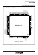
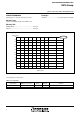
MITSUBISHI MICROCOMPUTERS 38C8 Group SINGLE-CHIP 8-BIT CMOS MICROCOMPUTER 73 75 74 77 76 84 83 82 81 80 79 78 87 86 85 91 90 89 88 93 92 95 94 97 96 101 100 99 98 109 72 110 71 111 112 70 69 68 67 66 113 114 115 116 65 64 63 62 117 118 119 120 121 122 123 124 125 126 61 60 59 58 57 56 55 M38C89MF-XXXFP 127 128 54 53 52 51 50 49 48 47 46 45 44 43 42 41 40 129 130 131 132 133 134 135 136 137 138 139 140 141 142 39 38 37 143 36 35 33 34 31 32 29 30 27 28 25 26 23 24 21 22 1
Fig.
MITSUBISHI MICROCOMPUTERS 38C8 Group SINGLE-CHIP 8-BIT CMOS MICROCOMPUTER PIN DESCRIPTION Table 1 Pin description Pin Name VCC, VSS RESET XIN Power source Reset input Clock input XOUT Clock output OSCSEL RC oscillation select Sub-clock input Sub-clock output XCIN XCOUT VLIN VL1 – VL5 COM0 – COM15 SEG0/COM16– SEG7/COM23, SEG60COM31– SEG67/COM24 SEG8–SEG59 P00–P07 P14–P17 P10/AIN4– P13/AIN7 P20–P27 P30/AIN0 – P33/AIN3 P40/INT0 Power source input for LCD LCD power source Common output Function exce
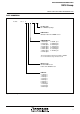
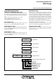
MITSUBISHI MICROCOMPUTERS 38C8 Group SINGLE-CHIP 8-BIT CMOS MICROCOMPUTER PART NUMBERING Product M38C8 9 M F –XXX FP Package type FP: 144P6Q-A package ROM number Omitted in One Time PROM version.
MITSUBISHI MICROCOMPUTERS 38C8 Group SINGLE-CHIP 8-BIT CMOS MICROCOMPUTER GROUP EXPANSION Packages Mitsubishi plans to expand the 38C8 group as follows. 144P6Q-A ................................... 0.5 mm-pitch plastic molded QFP Memory Type Support for mask ROM and One Time PROM versions Memory Size ROM/PROM size ............................................................ 60 K bytes RAM size ........................................................................
MITSUBISHI MICROCOMPUTERS 38C8 Group SINGLE-CHIP 8-BIT CMOS MICROCOMPUTER [Stack Pointer (S)] FUNCTIONAL DESCRIPTION CENTRAL PROCESSING UNIT (CPU) The accumulator is an 8-bit register. Data operations such as data transfer, etc., are executed mainly through the accumulator. The stack pointer is an 8-bit register used during subroutine calls and interrupts. This register indicates start address of stored area (stack) for storing registers during subroutine calls and interrupts.
MITSUBISHI MICROCOMPUTERS 38C8 Group SINGLE-CHIP 8-BIT CMOS MICROCOMPUTER On-going Routine Interrupt request (Note) M (S) Execute JSR Push return address on stack M (S) (PCH) (S) (S) – 1 M (S) (PCL) (S) (S)– 1 (S) M (S) (S) M (S) (S) Subroutine (S) (S) + 1 (PCL) M (S) (S) (S) + 1 (PCH) M (S) (S) – 1 (PCL) (PS) Push contents of processor status register on stack (S) – 1 Execute RTI Note: Condition for acceptance of an interrupt Push return address on stack (S) – 1 Interrupt Se
MITSUBISHI MICROCOMPUTERS 38C8 Group SINGLE-CHIP 8-BIT CMOS MICROCOMPUTER [Processor status register (PS)] The processor status register is an 8-bit register consisting of 5 flags which indicate the status of the processor after an arithmetic operation and 3 flags which decide MCU operation. Branch operations can be performed by testing the Carry (C) flag , Zero (Z) flag, Overflow (V) flag, or the Negative (N) flag. In decimal mode, the Z, V, N flags are not valid.
MITSUBISHI MICROCOMPUTERS 38C8 Group SINGLE-CHIP 8-BIT CMOS MICROCOMPUTER [CPU Mode Register (CPUM)] 003B16 The CPU mode register contains the stack page selection bit and the internal system clock selection bit. The CPU mode register is allocated at address 003B16.
MITSUBISHI MICROCOMPUTERS 38C8 Group SINGLE-CHIP 8-BIT CMOS MICROCOMPUTER MEMORY Special Function Register (SFR) Area The Special Function Register area in the zero page contains control registers such as I/O ports and timers. Zero Page Access to this area with only 2 bytes is possible in the zero page addressing mode. Special Page RAM RAM is used for data storage and for stack area of subroutine calls and interrupts.
MITSUBISHI MICROCOMPUTERS 38C8 Group SINGLE-CHIP 8-BIT CMOS MICROCOMPUTER 000016 Port P0 (P0) 000116 Port P0 direction register (P0D) 000216 Port P1 (P1) 000316 Port P1 direction register (P1D) 002016 Timer X (low-order) (TXL) 002116 Timer X (high-order) (TXH) 002216 Timer Y (low-order) (TYL) 002316 Timer Y (high-order) (TYH) 000416 Port P2 (P2) 000516 Port P2 direction register (P2D) 000616 Port P3 (P3) 000716 Port P3 direction register (P3D) 000916 Port P4 direction register (P4D) 002416 Timer 1 (T1)
MITSUBISHI MICROCOMPUTERS 38C8 Group SINGLE-CHIP 8-BIT CMOS MICROCOMPUTER I/O PORTS [Direction Registers] The I/O ports P0–P3 and P41–P47 have direction registers which determine the input/output direction of each individual pin. Each bit in a direction register corresponds to one pin, each pin can be set to be input port or output port. When “0” is written to the bit corresponding to a pin, that pin becomes an input pin. When “1” is written to that bit, that pin becomes an output pin.
MITSUBISHI MICROCOMPUTERS 38C8 Group SINGLE-CHIP 8-BIT CMOS MICROCOMPUTER Table 5 List of I/O port function Pin P00–P07 P10/AIN4– P13/AIN7 P14–P17 P20–P27 Name Port P0 Port P1 Input/Output Input/Output, individual bits I/O format CMOS compatible input level CMOS 3-state output Port P2 Input/Output, individual bits P30/AIN0– P33/AIN3 Port P3 Input/Output, individual bits CMOS compatible input level CMOS 3-state output CMOS compatible input level CMOS 3-state output Key input (key-on wake-up) inte
MITSUBISHI MICROCOMPUTERS 38C8 Group SINGLE-CHIP 8-BIT CMOS MICROCOMPUTER (2) Ports P10–P13, P3 (1) Ports P0, P14–P17, P2, P41 Pull-up control Pull-up control Direction register Direction register Data bus Port latch Data bus Port latch A-D converter input Analog input pin selection bit Key-on wake-up interrupt input INT1 interrupt input, ADT Except P0, P14–P17 (3) Port P40 Data bus INT0 interrupt input (4) Port P42 (5) Port P43 Pull-up control Pull-up control Direction register Data bus
MITSUBISHI MICROCOMPUTERS 38C8 Group SINGLE-CHIP 8-BIT CMOS MICROCOMPUTER (6) Port P44 (7) Port P45 Pull-up control Serial I/O enable bit Receive enalble bit Direction register Port latch Data bus Databus Serial I/O input (9) Port P47 Serial I/O synchronous clock selection bit Serial I/O enable bit Pull-up control Serial I/O mode selection bit Serial I/O enable bit Direction register Port latch Serial I/O ready output Serial I/O clock input Fig.
MITSUBISHI MICROCOMPUTERS 38C8 Group SINGLE-CHIP 8-BIT CMOS MICROCOMPUTER INTERRUPTS Interrupt Operation Interrupts occur by fourteen sources: five external, eight internal, and one software. By acceptance of an interrupt, the following operations are automatically performed: 1. The contents of the program counter and processor status register are automatically pushed onto the stack. 2. The interrupt disable flag is set and the corresponding interrupt request bit is cleared. 3.
MITSUBISHI MICROCOMPUTERS 38C8 Group SINGLE-CHIP 8-BIT CMOS MICROCOMPUTER Interrupt request bit Interrupt enable bit Interrupt disable flag (I) Interrupt request BRK instruction Reset Fig.
MITSUBISHI MICROCOMPUTERS 38C8 Group SINGLE-CHIP 8-BIT CMOS MICROCOMPUTER Key Input Interrupt (Key-on Wake-Up) A key input interrupt request is generated by applying “L” level to any pin of port P2 that have been set to input mode. In other words, it is generated when AND of input level goes from “1” to “0”.
MITSUBISHI MICROCOMPUTERS 38C8 Group SINGLE-CHIP 8-BIT CMOS MICROCOMPUTER TIMERS is set to “1”. Read and write operation on 16-bit timer must be performed for both high and low-order bytes. When reading a 16-bit timer, read the highorder byte first. When writing to a 16-bit timer, write the low-order byte first. The 16-bit timer cannot perform the correct operation when reading during the write operation, or when writing during the read operation.
MITSUBISHI MICROCOMPUTERS 38C8 Group SINGLE-CHIP 8-BIT CMOS MICROCOMPUTER Timer X Timer X is a 16-bit timer that can be selected in one of four modes and can be controlled the timer X write by setting the timer X mode register. (1) Timer Mode When the timer X count source selection bit is “0”, the timer counts f(XIN)/16 (or f(XCIN)/16 in low-speed mode). When it is “1”, the timer counts f(XIN). (2) Buzzer Output Mode When the timer X count source selection bit is “0”, the timer counts f(XCIN).
MITSUBISHI MICROCOMPUTERS 38C8 Group SINGLE-CHIP 8-BIT CMOS MICROCOMPUTER Timer Y Timer Y is a 16-bit timer that can be selected in one of four modes. (1) Timer Mode The timer counts f(XIN)/16 (or f(XCIN)/16 in low-speed mode). (2) Period Measurement Mode CNTR1 interrupt request is generated at rising/falling edge of CNTR1 pin input signal. Simultaneously, the value in timer Y latch is reloaded in timer Y and timer Y continues counting down.
MITSUBISHI MICROCOMPUTERS 38C8 Group SINGLE-CHIP 8-BIT CMOS MICROCOMPUTER Timer 1, Timer 2, Timer 3 Timer 1, timer 2, and timer 3 are 8-bit timers. The count source for each timer can be selected by the timer 123 mode register. The timer latch value is not affected by a change of the count source. However, because changing the count source may cause an inadvertent count down of the timer. Therefore, rewrite the value of timer whenever the count source is changed.
MITSUBISHI MICROCOMPUTERS 38C8 Group SINGLE-CHIP 8-BIT CMOS MICROCOMPUTER SERIAL I/O (1) Clock Synchronous Serial I/O Mode Serial I/O can be used as either clock synchronous or asynchronous (UART) serial I/O. A dedicated timer (baud rate generator) is also provided for baud rate generation. Clock synchronous serial I/O can be selected by setting the mode selection bit of the serial I/O control register to “1”. For clock synchronous serial I/O, the transmitter and the receiver must use the same clock.
MITSUBISHI MICROCOMPUTERS 38C8 Group SINGLE-CHIP 8-BIT CMOS MICROCOMPUTER (2) Asynchronous Serial I/O (UART) Mode but the two buffers have the same address in memory. Since the shift register cannot be written to or read from directly, transmit data is written to the transmit buffer, and receive data is read from the receive buffer. The transmit buffer can also hold the next data to be transmitted, and the receive buffer register can hold a character while the next character is being received.
MITSUBISHI MICROCOMPUTERS 38C8 Group SINGLE-CHIP 8-BIT CMOS MICROCOMPUTER [Transmit Buffer/Receive Buffer Register (TB/RB)] 001816 The transmit buffer register and the receive buffer register are located at the same address. The transmit buffer register is write-only and the receive buffer register is read-only. If a character bit length is 7 bits, the MSB of data stored in the receive buffer register is “0”.
MITSUBISHI MICROCOMPUTERS 38C8 Group SINGLE-CHIP 8-BIT CMOS MICROCOMPUTER b7 b7 b0 Serial I/O status register (SIOSTS : address 001916) b7 b0 Serial I/O control register (SIOCON : address 001A16) Transmit buffer empty flag (TBE) 0: Buffer full 1: Buffer empty BRG count source selection bit (CSS) 0: f(XIN) (f(XCIN) in low-speed mode) 1: f(XIN)/4 (f(XCIN)/4 in low-speed mode) Receive buffer full flag (RBF) 0: Buffer empty 1: Buffer full Transmit shift register shift completion flag (TSC) 0: Transmi
MITSUBISHI MICROCOMPUTERS 38C8 Group SINGLE-CHIP 8-BIT CMOS MICROCOMPUTER A-D CONVERTER [A-D Conversion Registers (ADL, ADH)] 003216, 003316 The A-D conversion registers are read-only registers that contain the result of an A-D conversion. During A-D conversion, do not read these registers. Resistor ladder The resistor ladder outputs the comparison voltage by dividing the voltage between VDD and VSS by resistance.
Bit 84 SEG58 133 SEG9 SEG8 Segment driver 134 14 15 Bit selector 7 8 Segment driver 0 1 Segment driver 14 15 Bit 14 15 Bit selector 7 8 SEG59 83 Segment driver 0 1 008316, 00C716 or 038316, 03C716 L M5 L M3 L M2 VL5 11 Voltage multiplier VL2 C1 C3 9 LCD control register 1 (address 003716) LCD control register 2 (address 003816) 5 COM0 COM1 6 74 142 141 73 Common/Segment driver f(XCIN)/16 f(XIN)/1024 COM15 COM16/ COM17/ COM31/ SEG60 SEG1 SEG0 Common driver “0” “1”
MITSUBISHI MICROCOMPUTERS 38C8 Group SINGLE-CHIP 8-BIT CMOS MICROCOMPUTER Table 7 Maximum number of display pixels at each duty ratio LCD Controller/Driver Function Duty ratio The controller/driver performs the bias control and the time sharing control by the LCD control registers 1, 2 (LC1, LC2), and the LCD mode register (LM). The data of corresponding LCDRAM is output from the segment pins according to the output timing of the common pins.
MITSUBISHI MICROCOMPUTERS 38C8 Group SINGLE-CHIP 8-BIT CMOS MICROCOMPUTER Bias Control Voltage Multiplier In the LCD power source pins (VL1–VL5), 1/7 bias is automatically generated in 32 duty ratio and 1/5 bias is done in 16 duty ratio as well. Be sure to connect the capacitor for smoothness to these pins. When requiring 1/5 bias in 32 duty ratio, use an external resistor to generate a necessary level. In this case the drivability selection bit 1 of LCD control register 1 must be “1”.
MITSUBISHI MICROCOMPUTERS 38C8 Group SINGLE-CHIP 8-BIT CMOS MICROCOMPUTER Common Pin and Duty Ratio Control LCD Display RAM The common pins (COM0–COM31) to be used are determined by duty ratio. Select duty ratio by the duty ratio selection bit (bit 0 of the LCD mode register). When LCD display RAM address selection bit is “0”, the area of addresses 034016 to 042F16 is the designated RAM for the LCD display. When the bit is “1”, the area of addresses 004016 to 012F16 is the designated RAM for it.
MITSUBISHI MICROCOMPUTERS 38C8 Group SINGLE-CHIP 8-BIT CMOS MICROCOMPUTER LCDCK 1 frame (16 clocks) 1 frame (16 clocks) VL5 VL4 COM23 VL3 VL2 VL1 VSS VL5 VL4 COM22 VL3 VL2 VL1 VSS VL5 VL4 SEG0 VL3 VL2 VL1 VSS VL5 VL4 VL3 VL2 VL1 SEG0 – COM23 VSS VL1 VL2 VL3 VL4 VL5 ON OFF ON OFF VL5 VL4 VL3 VL2 VL1 SEG0 – COM22 VSS VL1 VL2 VL3 VL4 VL5 OFF OFF Fig.
MITSUBISHI MICROCOMPUTERS 38C8 Group SINGLE-CHIP 8-BIT CMOS MICROCOMPUTER LCDCK 1 frame (32 clocks) COM31 1 frame (32 clocks) VL5 VL4 VL3 VL2 VL1 VSS VL5 VL4 VL3 COM30 VL2 VL1 VSS VL5 VL4 VL3 SEG0 VL2 VL1 VSS VL5 VL4 VL3 SEG0 – COM31 VL2 VL1 VSS VL1 VL2 VL3 VL4 VL5 ON OFF ON OFF ON OFF VL5 VL4 VL3 SEG0 – COM30 VL2 VL1 VSS VL1 VL2 VL3 VL4 VL5 OFF Fig.
MITSUBISHI MICROCOMPUTERS 38C8 Group SINGLE-CHIP 8-BIT CMOS MICROCOMPUTER RESET CIRCUIT To reset the microcomputer, RESET pin should be held at an “L” level for 2 µs or more. Then the RESET pin is returned to an “H” level (the power source voltage should be between VCC (min.) and 5.5 V, and the quartz-crystal oscillator should be stable), reset is released. After the reset is completed, the program starts from the address contained in address FFFD16 (high-order byte) and address FFFC16 (low-order byte).
MITSUBISHI MICROCOMPUTERS 38C8 Group SINGLE-CHIP 8-BIT CMOS MICROCOMPUTER Address Register contents Address (1) Port P0 direction register 000116 0016 (21) A-D control register 003116 0816 (2) Port P1 direction register 000316 0016 003216 XX16 (3) Port P2 direction register 000516 0016 003316 XX16 (4) Port P3 direction register 000716 0016 (22) A-D conversion register (low-order) (23) A-D conversion register (high-order) (24) LCD control register 1 003716 0016 (5) Port P4 directio
MITSUBISHI MICROCOMPUTERS 38C8 Group SINGLE-CHIP 8-BIT CMOS MICROCOMPUTER CLOCK GENERATING CIRCUIT The 38C8 group has two built-in oscillation circuits: main clock XINXOUT oscillation circuit and sub-clock XCIN-XCOUT oscillation circuit. An oscillation circuit can be formed by connecting a resonator between XIN and XOUT (XCIN and XCOUT). RC oscillation is available for XIN-XOUT.
MITSUBISHI MICROCOMPUTERS 38C8 Group SINGLE-CHIP 8-BIT CMOS MICROCOMPUTER XCOUT XCIN XIN XOUT Timer 1 count source selection bit Internal system clock selection bit (Note) Low-speed mode “1” 1/2 “0” Middle-/High-speed mode Timer 2 count source selection bit “1” 1/2 1/4 Timer 1 “0” “0” Timer 2 “1” Main clock division ratio selection bit Middle-speed mode “1” Main clock stop bit Q S S R STP instruction Timing φ (Internal clock) “0” High-speed mode or Low-speed mode WIT instruction R Q
MITSUBISHI MICROCOMPUTERS 38C8 Group SINGLE-CHIP 8-BIT CMOS MICROCOMPUTER Reset “0 ” “0” 6 ” “0 “1 ” 6 ” “1 CM6 Middle-speed mode (f(φ) = 0 .
MITSUBISHI MICROCOMPUTERS 38C8 Group SINGLE-CHIP 8-BIT CMOS MICROCOMPUTER NOTES ON PROGRAMMING Processor Status Register A-D Converter The contents of the interrupt request bits do not change immediately after they have been written. After writing to an interrupt request register, execute at least one instruction before performing a BBC or BBS instruction. The comparator is constructed linked to a capacitor.
MITSUBISHI MICROCOMPUTERS 38C8 Group SINGLE-CHIP 8-BIT CMOS MICROCOMPUTER NOTES ON USE Countermeasures Against Noise Noise (1) Shortest wiring length ➀ Wiring for RESET pin Make the length of wiring which is connected to the RESET pin as short as possible. Especially, connect a capacitor across the RESET pin and the VSS pin with the shortest possible wiring (within 20mm). ● Reason The width of a pulse input into the RESET pin is determined by the timing necessary conditions.
MITSUBISHI MICROCOMPUTERS 38C8 Group SINGLE-CHIP 8-BIT CMOS MICROCOMPUTER (3) Oscillator concerns In order to obtain the stabilized operation clock on the user system and its condition, contact the oscillator manufacturer and select the oscillator and oscillation circuit constants. Be careful especially when range of voltage or/and temperature is wide. Also, take care to prevent an oscillator that generates clocks for a microcomputer operation from being affected by other signals.
MITSUBISHI MICROCOMPUTERS 38C8 Group SINGLE-CHIP 8-BIT CMOS MICROCOMPUTER DATA REQUIRED FOR MASK ORDERS ROM PROGRAMMING METHOD The following are necessary when ordering a mask ROM production: 1. Mask ROM Order Confirmation Form✽ 2. Mark Specification Form✽ 3. Data to be written to ROM, in EPROM form (three identical copies) or one floppy disk.
MITSUBISHI MICROCOMPUTERS 38C8 Group SINGLE-CHIP 8-BIT CMOS MICROCOMPUTER ELECTRICAL CHARACTERISTICS Table 11 Absolute maximum ratings VI VI VI Parameter Power source voltage Input voltage P00–P07, P10–P17, P20–P27, P30–P33, P40–P47 Input voltage C1, C2 Input voltage RESET, XIN, XCIN Input voltage VLIN VI VO Input voltage Output voltage Symbol VCC VI VO VO VO Pd Topr Tstg VL1, VL2, VL3, VL4, VL5 P00–P07, P10–P17, P20–P27, P30–P33, P41–P47 Output voltage C1, C2, C3 Output voltage COM0–COM31, SEG0–SE
MITSUBISHI MICROCOMPUTERS 38C8 Group SINGLE-CHIP 8-BIT CMOS MICROCOMPUTER Table 13 Recommended operating conditions (mask ROM version) (Vcc = 2.2 to 5.5 V, Ta = –20 to 85°C, unless otherwise noted) Symbol f(CNTR0) f(CNTR1) f(XIN) f(XCIN) Parameter Conditions Min. Limits Typ. Timer X, timer Y input frequency (duty cycle 50%) Main clock input oscillation frequency (Note 1) High-speed mode (4.0 V ≤ VCC ≤ 5.5 V) High-speed mode (2.2 V ≤ VCC < 4.0 V) Middle-speed mode (2.7 V ≤ VCC ≤ 5.
MITSUBISHI MICROCOMPUTERS 38C8 Group SINGLE-CHIP 8-BIT CMOS MICROCOMPUTER Table 15 Electrical characteristics (Vcc = 2.2 to 5.
MITSUBISHI MICROCOMPUTERS 38C8 Group SINGLE-CHIP 8-BIT CMOS MICROCOMPUTER Table 16 Electrical characteristics (Vcc = 2.2 to 5.5 V, Ta = –20 to 85°C, unless otherwise noted) Symbol VRAM ICC IAD IL5 FROSC Parameter RAM hold voltage Power source current A-D converter current dissipation VL5 input current (Note) RC oscillation frequency Test conditions When clock is stopped High-speed mode, Vcc = 5.0 V f(XIN) = 8.0 MHz f(XCIN) = 32.768 kHz Middle-speed mode, Vcc = 5.0 V f(XIN) = 8.0 MHz f(XCIN) = 32.
MITSUBISHI MICROCOMPUTERS 38C8 Group SINGLE-CHIP 8-BIT CMOS MICROCOMPUTER Table 17 A-D converter characteristics (Vcc = 2.2 to 5.5 V, Vss = 0 V, Ta = –20 to 85°C, f(XIN) ≤ 4 MHz, in middle-speed/high-speed mode) Symbol — — tconv IIA Parameter Test conditions Resolution Absolute accuracy (excluding quantization error) Conversion time Analog port input current Limits Typ. Min. VCC = 2.7–5.5 V VCC = 2.5–2.7 V (Ta = –10 to 50 °C) f(XIN) = 4 MHz (Note) 30.5 0.5 Max. 10 ±4 ±6 34 5.
MITSUBISHI MICROCOMPUTERS 38C8 Group SINGLE-CHIP 8-BIT CMOS MICROCOMPUTER Table 20 Timing requirements 2 (One Time PROM version) (Vcc = 2.5 to 4.0 V, Vss = 0 V, Ta = –20 to 85°C, unless otherwise noted) Symbol tw(RESET) tc(XIN) twH(XIN) twL(XIN) tc(CNTR) twH(CNTR) twL(CNTR) twH(INT) twL(INT) tc(SCLK) twH(SCLK) twL(SCLK) tsu(RxD-SCLK) th(SCLK-RxD) Parameter Reset input “L” pulse width Main clock input cycle time (XIN input) Vcc = 2.7 to 4.0 V Main clock input cycle time (XIN input) Vcc = 2.5 to 2.
MITSUBISHI MICROCOMPUTERS 38C8 Group SINGLE-CHIP 8-BIT CMOS MICROCOMPUTER Table 21 Switching characteristics 1 (Vcc = 4.0 to 5.
MITSUBISHI MICROCOMPUTERS 38C8 Group SINGLE-CHIP 8-BIT CMOS MICROCOMPUTER tC(CNTR) tWL(CNTR) tWH(CNTR) CNTR0, CNTR1 0.8VCC 0.2VCC tWL(INT) tWH(INT) INT0, INT1 0.8VCC 0.2VCC tW(RESET) RESET 0.8VCC 0.2VCC tC(XIN) tWL(XIN) tWH(XIN) 0.8VCC XIN 0.2VCC tC(SCLK) tf SCLK tWL(SCLK) tr tWH(SCLK) 0.8VCC 0.2VCC tsu(RXD-SCLK) th(SCLK-RXD) 0.8VCC 0.2VCC R XD td(SCLK-TXD) tv(SCLK-TXD) T XD Fig.
MITSUBISHI MICROCOMPUTERS 38C8 Group SINGLE-CHIP 8-BIT CMOS MICROCOMPUTER PACKAGE OUTLINE MMP EIAJ Package Code LQFP144-P-2020-0.50 Plastic 144pin 20✕20mm body LQFP Weight(g) 1.23 JEDEC Code – Lead Material Cu Alloy MD e 144P6Q-A b2 D 144 ME HD 109 1 l2 Recommended Mount Pad 108 36 A A1 A2 b c D E e HD HE L L1 Lp HE E Symbol 73 37 72 A L1 F e x M L Detail F Lp c b A1 y A3 A2 A3 x y b2 I2 MD ME Dimension in Millimeters Min Nom Max – – 1.7 0.125 0.2 0.05 – – 1.4 0.
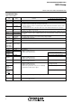
REVISION HISTORY Rev. 38C8 GROUP DATA SHEET Date Description Summary Page 1.0 01/18/01 1.1 03/21/01 First Edition 2 3 4 14 17 26 33 34 37 37 40 41 42 42 Figure 1 is partly revised. Figure 2 is partly revised. Pin name into Table 1 is partly revised. Pin name into Table 5 is partly revised. Explanations of “Interrupt Operation” are partly eliminated. Address of [Baud Rate Generator (BRG)] is revised. Figure name of Figure 31 is partly revised. Figure name of Figure 32 is partly revised.
REVISION HISTORY Rev. 38C8 GROUP DATA SHEET Date Description Summary Page 1.4 06/25/02 15 17 19 20 20 21 25 30 31 31 32 35 37 38 39 40 41, 42 44 46 47 (1) in Figure 11 is partly revised. Some source numbers in “[INTERRUPTS]” are corrected. Figure 15 is partly revised. The mode name (buzzer output mode) in Figure 16 is corrected.The mode name of bit 6 in Figure 17 is corrected. Explanations of “[(2) Buzzer Output Mode]” are partly added. f(XCIN) in Figure 22 is added.