7540 Group REJ03B0011-0400 Rev.4.00 Jun 21, 2004 SINGLE-CHIP 8-BIT CMOS MICROCOMPUTER DESCRIPTION The 7540 Group is the 8-bit microcomputer based on the 740 family core technology. The 7540 Group has a serial I/O, 8-bit timers, a 16-bit timer, and an A/D converter, and is useful for control of home electric appliances and office automation equipment. FEATURES • • • • • • • • • • • • • • Basic machine-language instructions ......................................
7540 Group P07 P10/RXD1 P11/TXD1 P12/SCLK1/SCLK2 P13/SRDY1/SDATA2 P14/CNTR0 P20/AN0 P21/AN1 25 26 27 28 29 30 31 18 17 20 19 22 21 23 24 P06 P05 P04 P03/TXOUT P02/TZOUT P01/TYOUT P00/CNTR1 P37/INT0 PIN CONFIGURATION (TOP VIEW) M37540Mx-XXXGP M37540MxT-XXXGP M37540MxV-XXXGP M37540ExGP M37540E8T-XXXGP M37540E8V-XXXGP 16 15 14 13 12 11 10 9 7 8 6 5 4 3 2 P22/AN2 P23/AN3 P24/AN4 P25/AN5 VREF RESET CNVSS VCC 1 32 P34(LED4) P33(LED3) P32(LED2) P31(LED1) P30(LED0) VSS XOUT XIN Package typ
7540 Group P12/SCLK1/SCLK2 P13/SRDY1/SDATA2 P14/CNTR0 1 32 P11/TXD1 3 30 P10/RXD1 P07 P20/AN0 4 29 P06 P21/AN1 P22/AN2 5 28 P23/AN3 P24/AN4 7 P05 P04 P03/TXOUT P02/TZOUT P25/AN5 VREF 9 6 8 M37540Mx-XXXSP M37540ExSP 2 31 27 26 25 23 P01/TYOUT P00/CNTR1 22 P37/INT0 21 P34(LED4) 13 20 14 14 19 P33(LED3) P32(LED2) XOUT 15 18 P31(LED1) VSS 16 17 P30(LED0) 10 RESET CNVSS VCC XIN 11 12 24 Package type: 32P4B Fig.
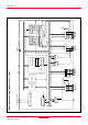
Fig. 5 Functional block diagram (32P6U package) Rev.4.
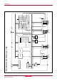
Fig. 6 Functional block diagram (36P2R package) Rev.4.
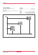
Fig. 7 Functional block diagram (32P4B package) Rev.4.
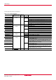
540 Group PIN DESCRIPTION Table 1 Pin description Pin Name Vcc, Vss Power source (Note 1) VREF Analog reference voltage CNVss CNVss RESET Reset input XIN Clock input XOUT Clock output P00/CNTR1 P01/TYOUT P02/TZOUT P03/TXOUT P04–P07 I/O port P0 P10/RxD1 I/O port P1 P11/TxD1 P12/SCLK1/SCLK2 P13/SRDY1/SDATA2 P14/CNTR0 P20/AN0–P27/AN7 I/O port P2 (Note 2) P30–P35 I/O port P3 (Note 3) P36/INT1 P37/INT0 Function •Apply voltage of 2.2 to 5.5 V to Vcc, and 0 V to Vss.
7540 Group GROUP EXPANSION Renesas plans to expand the 7540 group as follow: Memory type Support for Mask ROM version, One Time PROM version, and Emulator MCU . Memory size ROM/PROM size ................................................. 8 K to 32 K bytes RAM size .............................................................. 384 to 768 bytes Package 32P4B .................................................. 32-pin plastic molded SDIP 32P6U-A ...................... 0.
7540 Group Currently supported products are listed below.
7540 Group FUNCTIONAL DESCRIPTION Stack pointer (S) Central Processing Unit (CPU) The MCU uses the standard 740 family instruction set. Refer to the table of 740 family addressing modes and machine-language instructions or the SERIES 740 USER’S MANUAL for details on each instruction set. Machine-resident 740 family instructions are as follows: 1. The FST and SLW instructions cannot be used. 2. The MUL and DIV instructions can be used. 3. The WIT instruction can be used. 4.
7540 Group On-going Routine Interrupt request (Note) M (S) Execute JSR M (S) Store Return Address on Stack (S) (PC H) (S) (S – 1) M (S) (PCL) (S) (S – 1) M (S) Subroutine Restore Return Address (S + 1) (PCL) M (S) (S) (S + 1) (PCH) M (S) (S – 1) (PC L) (S) (S – 1) M (S) (PS) (S) (S – 1) Interrupt Service Routine Execute RTS (S) (PC H) Execute RTI Note : The condition to enable the interrupt (S) (S + 1) (PS) M (S) (S) (S + 1) (PC L) M (S) (S) (S + 1) (PC H) M (S)
7540 Group Processor status register (PS) The processor status register is an 8-bit register consisting of flags which indicate the status of the processor after an arithmetic operation. Branch operations can be performed by testing the Carry (C) flag, Zero (Z) flag, Overflow (V) flag, or the Negative (N) flag. In decimal mode, the Z, V, N flags are not valid. After reset, the Interrupt disable (I) flag is set to “1”, but all other flags are undefined.
7540 Group [CPU mode register] CPUM The CPU mode register contains the stack page selection bit. This register is allocated at address 003B16. b7 b0 CPU mode register (CPUM: address 003B16, initial value: 8016) Switching method of CPU mode register Switch the CPU mode register (CPUM) at the head of program after releasing Reset in the following method.
7540 Group Memory Special function register (SFR) area The SFR area in the zero page contains control registers such as I/O ports and timers. RAM RAM is used for data storage and for a stack area of subroutine calls and interrupts. ROM The first 128 bytes and the last 2 bytes of ROM are reserved for device testing and the rest is a user area for storing programs. Interrupt vector area The interrupt vector area contains reset and interrupt vectors.
7540 Group 000016 Port P0 (P0) 002016 Timer Y, Z mode register (TYZM) 000116 Port P0 direction register (P0D) 002116 Prescaler Y (PREY) 000216 Port P1 (P1) 002216 Timer Y secondary (TYS) 000316 Port P1 direction register (P1D) 002316 Timer Y primary (TYP) 000416 Port P2 (P2) 002416 Timer Y, Z waveform output control register (PUM) 000516 Port P2 direction register (P2D) 002516 Prescaler Z (PREZ) 000616 Port P3 (P3) 002616 Timer Z secondary (TZS) 000716 Port P3 direction registe
7540 Group I/O Ports [Direction registers] PiD The I/O ports have direction registers which determine the input/ output direction of each pin. Each bit in a direction register corresponds to one pin, and each pin can be set to be input or output. When “1” is set to the bit corresponding to a pin, this pin becomes an output port. When “0” is set to the bit, the pin becomes an input port. When data is read from a pin set to output, not the value of the pin itself but the value of port latch is read.
7540 Group Table 5 I/O port function table Pin P00/CNTR1 P01/TYOUT P02/TZOUT P03/TXOUT P04–P07 Name Input/output I/O format I/O port P0 I/O individual •CMOS compatible bits input level •CMOS 3-state output (Note 1) Non-port function Key input interrupt Timer X function output Timer Y function output Timer Z function output Timer A function input P10/RxD1 P11/TxD1 P12/SCLK1/SCLK2 P13/SRDY1/SDATA2 P14/CNTR0 P20/AN0– P27/AN7 P30–P35 P36/INT1 P37/INT0 I/O port P1 Serial I/O1 function input/output Serial I
7540 Group (1)Port P00 (2)Ports P01, P02 Pull-up control Pull-up control Direction register Direction register Data bus Port latch Data bus Port latch ** Programmable waveform generation mode Timer output CNTR1 interrupt input To key input interrupt generating circuit P00 key-on wakeup selection bit (3)Port P03 To key input interrupt generating circuit (4)Ports P04–P07 Pull-up control Pull-up control Direction register Data bus Direction register Data bus Port latch Port latch Timer
7540 Group (8) Port P13 (9) Port P14 SDATA2 output in operation signal SDATA2 pin selection bit Direction register Serial I/O mode selection bit Serial I/O1 enable bit SRDY1 output enable bit Direction register Data bus Data bus Port latch Port latch Pulse output mode Timer output P10, P12, P13 input level selection bit CNTR0 interrupt input Serial I/O1 ready output Serial I/O2 output Serial I/O2 input * (11) Ports P30–P35 (10) Ports P20–P27 Direction register Pull-up control Direction registe
7540 Group Interrupts Interrupts occur by 15 different sources : 5 external sources, 9 internal sources and 1 software source. Interrupt control All interrupts except the BRK instruction interrupt have an interrupt request bit and an interrupt enable bit, and they are controlled by the interrupt disable flag. When the interrupt enable bit and the interrupt request bit are set to “1” and the interrupt disable flag is set to “0”, an interrupt is accepted.
7540 Group Interrupt request bit Interrupt enable bit Interrupt disable flag I BRK instruction Reset Interrupt request Fig.
7540 Group Key Input Interrupt (Key-On Wake-Up) A key-on wake-up interrupt request is generated by applying “L” level to any pin of port P0 that has been set to input mode. In other words, it is generated when the AND of input level goes from “1” to “0”. An example of using a key input interrupt is shown in Figure 21, where an interrupt request is generated by pressing one of the keys provided as an active-low key matrix which uses ports P00 to P03 as input ports.
7540 Group Timers ●Timer A The 7540 Group has 5 timers: timer 1, timer A, timer X, timer Y and timer Z. The division ratio of every timer and prescaler is 1/(n+1) provided that the value of the timer latch or prescaler is n. All the timers are down count timers. When a timer reaches “0”, an underflow occurs at the next count pulse, and the corresponding timer latch is reloaded into the timer. When a timer underflows, the interrupt request bit corresponding to each timer is set to “1”.
7540 Group (3) Event counter mode Timer A counts signals input from the P00/CNTR1 pin. Except for this, the operation in event counter mode is the same as in timer mode. The active edge of CNTR 1 pin input signal can be selected from rising or falling by the CNTR1 active edge switch bit . (4) Pulse width HL continuously measurement mode In the pulse width HL continuously measurement mode, the pulse width (“H” and “L” levels) input to the P00/CNTR1 pin is measured.
7540 Group (4) Pulse width measurement mode In the pulse width measurement mode, the pulse width of the signal input to P14/CNTR0 pin is measured. The operation of Timer X can be controlled by the level of the signal input from the CNTR0 pin. When the CNTR0 active edge switch bit is “0”, the signal selected by the timer X count source selection bit is counted while the input signal level of CNTR0 pin is “H”. The count is stopped while the pin is “L”.
7540 Group ●Timer Y Timer Y is an 8-bit timer and counts the prescaler Y output. When Timer Y underflows, the timer Y interrupt request bit is set to “1”. Prescaler Y is an 8-bit prescaler and counts the signal selected by the timer Y count source selection bit. Prescaler Y has the prescaler Y latch to retain the reload value. Timer Y has the timer Y primary latch and timer Y secondary latch to retain the reload value. The value of prescaler Y latch is set to Prescaler Y when Prescaler Y underflows.
7540 Group ■ Notes on programmable generation waveform mode • Count set value In the programmable waveform generation mode, values of TYS, EXPYP, and EXPYS are valid by writing to TYP because the setting to them is executed all at once by writing to TYP. Even when changing TYP is not required, write the same value again.
7540 Group ●Timer Z Timer Z is an 8-bit timer and counts the prescaler Z output. When Timer Z underflows, the timer Z interrupt request bit is set to “1”. Prescaler Z is an 8-bit prescaler and counts the signal selected by the timer Z count source selection bit. Prescaler Z has the prescaler Z latch to retain the reload value. Timer Z has the timer Z primary latch and timer Z secondary latch to retain the reload value. The value of prescaler Z latch is set to Prescaler Z when Prescaler Z underflows.
7540 Group Notes on the programmable waveform generation mode are described below; ■ Notes on programmable waveform generation mode • Count set value In the programmable waveform generation mode, values of TZS, EXPZP, and EXPZS are valid by writing to TZP because the setting to them is executed all at once by writing to TZP. Even when changing TZP is not required, write the same value again.
7540 Group (4) Programmable wait one-shot generation mode In the programmable wait one-shot generation mode, the one-shot pulse by the setting value of timer Z secondary can be output from TZOUT pin by software or external trigger to INT0 pin after the wait by the setting value of the timer Z primary. When using this mode, be sure to set “1” to the timer Z write control bit to select “write to latch only”. Also, set the port P0 2 direction registers to output mode.
7540 Group b7 b0 Timer Y, Z mode register (TYZM : address 0020 16, initial value: 00 16) Timer Y operating mode bit 0 : Timer mode 1 : Programmable waveform generation mode Not used (return “0” when read) Timer Y write control bit 0 : Write to latch and timer simultaneously 1 : Write to only latch Timer Y count stop bit 0 : Count start 1 : Count stop Timer Z operating mode bits b5 b4 0 0 : Timer mode 0 1 : Programmable waveform generation mode 1 0 : Programmable one-shot generation mode 1 1 : Programmabl
7540 Group Data bus Timer 1 latch (8) Prescaler 1 latch (8) Prescaler 1 (8) f(XIN)/16 Timer 1 (8) Timer 1 interrupt request bit Pulse width HL continuously measurement mode Rising edge detected Period measurement mode Falling edge detected P00/CNTR1 CNTR1 active edge switch bit Data bus Timer A (low-order) latch (8) Timer A (low-order) (8) f(XIN)/16 Timer A operation mode bit Timer A count stop bit Fig. 28 Block diagram of timer 1 and timer A Rev.4.
7540 Group Data bus f(XIN)/16 f(XIN)/2 f(XIN) Timer X count source selection bits CNTR0 active edge switch bit “0” P14/CNTR0 Prescaler X latch (8) Timer X latch (8) Prescaler X (8) Timer X (8) Pulse width Timer mode measurement Pulse output mode mode Event counter mode Timer X count stop bit CNTR0 interrupt request bit “1” CNTR0 active “1” edge switch bit Q Toggle flip-flop T Q R “0” Port P14 latch Port P14 direction register Timer X interrupt request bit Writing to timer X latch Pulse
7540 Group Serial I/O ●Serial I/O1 (1) Clock Synchronous Serial I/O Mode Clock synchronous serial I/O1 mode can be selected by setting the serial I/O1 mode selection bit of the serial I/O1 control register (bit 6) to “1”. For clock synchronous serial I/O1, the transmitter and the receiver must use the same clock. If an internal clock is used, transfer is started by a write signal to the TB/RB. Serial I/O1 can be used as either clock synchronous or asynchronous (UART) serial I/O.
7540 Group The transmit and receive shift registers each have a buffer, but the two buffers have the same address in memory. Since the shift register cannot be written to or read from directly, transmit data is written to the transmit buffer register, and receive data is read from the receive buffer register. The transmit buffer register can also hold the next data to be transmitted, and the receive buffer register can hold a character while the next character is being received.
7540 Group [Transmit buffer register/receive buffer register (TB/RB)] 001816 The transmit buffer register and the receive buffer register are located at the same address. The transmit buffer is write-only and the receive buffer is read-only. If a character bit length is 7 bits, the MSB of data stored in the receive buffer is “0”.
7540 Group b7 b0 Serial I/O1 status register (SIO1STS : address 0019 16, initial value: 00 16) Transmit buffer empty flag (TBE) 0: Buffer full 1: Buffer empty Receive buffer full flag (RBF) 0: Buffer empty 1: Buffer full Transmit shift completion flag (TSC) 0: Transmit shift in progress 1: Transmit shift completed Overrun error flag (OE) 0: No error 1: Overrun error Parity error flag (PE) 0: No error 1: Parity error Framing error flag (FE) 0: No error 1: Framing error Summing error flag (SE) 0: (OE) U (P
7540 Group ●Serial I/O2 The serial I/O2 function can be used only for clock synchronous serial I/O. For clock synchronous serial I/O2 the transmitter and the receiver must use the same clock. When the internal clock is used, transfer is started by a write signal to the serial I/O2 register. Note: Serial I/O2 can be used in the following cases; (1) Serial I/O1 is not used, (2) Serial I/O1 is used as UART and BRG output divided by 16 is selected as the synchronized clock.
7540 Group Serial I/O2 operation By writing to the serial I/O2 register (address 003116) the serial I/ O2 counter is set to “7”. After writing, the SDATA2 pin outputs data every time the transfer clock shifts from “H” to “L”. And, as the transfer clock shifts from “L” to “H”, the SDATA2 pin reads data, and at the same time the contents of the serial I/O2 register are shifted by 1 bit.
7540 Group A/D Converter (2) When V REF voltage is lower than [3.0 V], the accuracy at the low temperature may become extremely low compared with that at room temperature When the system would be used at low temperature, the use at V REF =3.0 V or more is recommended. The functional blocks of the A/D converter are described below. [A/D conversion register] AD The A/D conversion register is a read-only register that stores the result of A/D conversion.
7540 Group Watchdog Timer The watchdog timer gives a means for returning to a reset status when the program fails to run on its normal loop due to a runaway. The watchdog timer consists of an 8-bit watchdog timer H and an 8-bit watchdog timer L, being a 16-bit counter. Standard operation of watchdog timer The watchdog timer stops when the watchdog timer control register (address 0039 16) is not set after reset.
7540 Group Reset Circuit Poweron The microcomputer is put into a reset status by holding the RESET pin at the “L” level for 2 µs or more when the power source voltage is 2.2 to 5.5 V and XIN is in stable oscillation. After that, this reset status is released by returning the RESET pin to the “H” level. The program starts from the address having the contents of address FFFD16 as high-order address and the contents of address FFFC16 as low-order address.
7540 Group Address (1) Port P0 direction register 000116 (2) Port P1 direction register 000316 Register contents 0016 X X X 0 0 (3) Port P2 direction register 000516 0016 (4) Port P3 direction register 000716 0016 (5) Pull-up control register 001616 0016 (6) Port P1P3 control register 001716 0016 (7) Serial I/O1 status register 001916 1 0 0 0 0 001A16 (9) UART control register 001B16 (10) Timer A mode register 001D16 0016 (11) Timer A (low-order) 001E16 FF16 (12) Timer
7540 Group Clock Generating Circuit An oscillation circuit can be formed by connecting a resonator between XIN and XOUT, and an RC oscillation circuit can be formed by connecting a resistor and a capacitor. Use the circuit constants in accordance with the resonator manufacturer's recommended values. Note: Externally connect a M37540 XI N XOUT Rd (1) On-chip oscillator operation When the MCU operates by the on-chip oscillator for the main clock, connect XIN pin to VSS and leave XOUT pin open.
7540 Group (1) Oscillation control • Stop mode When the STP instruction is executed, the internal clock φ stops at an “H” level and the XIN oscillator stops. At this time, timer 1 is set to “0116” and prescaler 1 is set to “FF16” when the oscillation stabilization time set bit after release of the STP instruction is “0”. On the other hand, timer 1 and prescaler 1 are not set when the above bit is “1”. Accordingly, set the wait time fit for the oscillation stabilization time of the oscillator to be used.
7540 Group XIN XOUT Rf Clock division ratio selection bit Middle-, high-, low-speed mode 1/2 Timer 1 Prescaler 1 1/2 1/4 On-chip oscillator mode Clock division ratio selection bit Middle-speed mode Timing φ (Internal clock) High-speed mode Double-speed mode RING 1/8 On-chip oscillator On-chip oscillator mode Q S Q S WIT instruction STP instruction R S Q R RESET R STP instruction Reset Interrupt disable flag l Interrupt request Fig.
7540 Group Stop mode Wait mode Interrupt WIT instruction Interrupt STP instruction State 1 Operation clock source: f(XIN) (Note 1) f(XIN) oscillation enabled On-chip oscillator stop CPUM3←02 CPUM3←12 Interrupt WIT instruction State 2 CPUM76←102 Operation clock source: f(XIN) (Note 1) f(XIN) oscillation enabled On-chip oscillator enabled CPUM76←002 State 3 Operation clock source: On-chip oscillator (Note 3) f(XIN) oscillation enabled On-chip oscillator enalbed 012 112 (Note 2) MISRG1←12 MISRG1←02 M
7540 Group NOTES ON PROGRAMMING State transition Processor Status Register Do not stop the clock selected as the operation clock because of setting of CM3, 4. The contents of the processor status register (PS) after reset are undefined except for the interrupt disable flag I which is “1”. After reset, initialize flags which affect program execution. In particular, it is essential to initialize the T flag and the D flag because of their effect on calculations.
7540 Group NOTES ON PERIPHERAL FUNCTIONS ■ Interrupt • Timer Y write mode When using this mode, be sure to set “1” to the timer Y write control bit to select “write to latch only”. When setting the followings, the interrupt request bit may be set to “1”.
7540 Group ■ Timer Z: Programmable Wait One-shot Generation Mode • Count set value In the programmable wait one-shot generation mode, values of TZS, EXPZP and EXPZS are valid by writing to TZP. Even when changing TZP is not required, write the same value again.
7540 Group ■ Note on Power Source Voltage ROM PROGRAMMING METHOD When the power source voltage value of a microcomputer is less than the value which is indicated as the recommended operating conditions, the microcomputer does not operate normally and may perform unstable operation.
7540 Group ELECTRICAL CHARACTERISTICS 1.
7540 Group Recommended Operating Conditions (General purpose) Table 9 Recommended operating conditions (1) (VCC = 2.2 to 5.
7540 Group Recommended Operating Conditions (General purpose)(continued) Table 10 Recommended operating conditions (2) (VCC = 2.2 to 5.5 V, Ta = –20 to 85 °C, unless otherwise noted) Symbol IOH(peak) IOL(peak) IOL(peak) IOH(avg) IOL(avg) IOL(avg) f(XIN) Limits Parameter Min.
7540 Group Electrical Characteristics (General purpose) Table 11 Electrical characteristics (1) (VCC = 2.2 to 5.
7540 Group Electrical Characteristics (General purpose)(continued) Table 12 Electrical characteristics (2) (VCC = 2.2 to 5.5 V, VSS = 0 V, Ta = –20 to 85 °C, unless otherwise noted) Limits Symbol ICC Parameter Power source current Test conditions One Time PROM version Mask ROM version Rev.4.00 Jun 21, 2004 REJ03B0011-0400Z page 56 of 82 High-speed mode, f(XIN) = 8 MHz Output transistors “off” High-speed mode, f(XIN) = 2 MHz, VCC = 2.
7540 Group A/D Converter Characteristics (General purpose) Table 13 A/D Converter characteristics (VCC = 2.7 to 5.
7540 Group Timing Requirements (General purpose) Table 14 Timing requirements (1) (VCC = 4.0 to 5.
7540 Group Table 16 Timing requirements (3) (VCC = 2.2 to 5.
7540 Group Switching Characteristics (General purpose) Table 17 Switching characteristics (1) (VCC = 4.0 to 5.
7540 Group Table 19 Switching characteristics (3) (VCC = 2.2 to 5.
7540 Group tC(CNTR0) tWL(CNTR0) tWH(CNTR0) CNTR0 0.8VCC 0.2VCC tC(CNTR1) tWL(CNTR1) tWH(CNTR1) 0.8VCC CNTR1 0.2VCC tWL(CNTR0) tWH(CNTR0) INT0, INT1 0.8VCC 0.2VCC tW(RESET) RESET 0.8VCC 0.2VCC tC(XIN) tWL(XIN) tWH(XIN) 0.8VCC XIN tC(SCLK1) tr tf SCLK1 0.2VCC tWL(SCLK1) tWH(SCLK1 ) 0.8VCC 0.2VCC tsu(RxD1-SCLK1) th(SCLK1 -RxD1) 0.8VCC 0.2VCC RXD1 (at receive) td(SCLK1 -TxD1) tv(SCLK1-TxD1) TXD1 (at transmit) tC(SCLK2) tr tf SCLK2 tWL(SCLK2) 0.
7540 Group ELECTRICAL CHARACTERISTICS 2.
7540 Group Recommended Operating Conditions (Extended operating temperature version) Table 21 Recommended operating conditions (1) (VCC = 2.4 to 5.
7540 Group Recommended Operating Conditions (Extended operating temperature version)(continued) Table 22 Recommended operating conditions (2) (VCC = 2.4 to 5.5 V, Ta = –40 to 85 °C, unless otherwise noted) Limits Symbol Parameter Min.
7540 Group Electrical Characteristics (Extended operating temperature version) Table 23 Electrical characteristics (1) (VCC = 2.4 to 5.
7540 Group Electrical Characteristics (Extended operating temperature version)(continued) Table 24 Electrical characteristics (2) (VCC = 2.4 to 5.5 V, VSS = 0 V, Ta = –40 to 85 °C, unless otherwise noted) Limits Symbol ICC Test conditions One Time PROM version High-speed mode, f(XIN) = 8 MHz Output transistors “off” High-speed mode, f(XIN) = 2 MHz, VCC = 2.
7540 Group A/D Converter Characteristics (Extended operating temperature version) Table 25 A/D Converter characteristics (VCC = 2.7 to 5.
7540 Group Timing Requirements (Extended operating temperature version) Table 26 Timing requirements (1) (VCC = 4.0 to 5.
7540 Group Switching Characteristics (Extended operating temperature version) Table 28 Switching characteristics (1) (VCC = 4.0 to 5.
7540 Group tC(CNTR0) tWL(CNTR0) tWH(CNTR0) CNTR0 0.8VCC 0.2VCC tC(CNTR1) tWL(CNTR1) tWH(CNTR1) 0.8VCC CNTR1 0.2VCC tWL(CNTR0) tWH(CNTR0) INT0, INT1 0.8VCC 0.2VCC tW(RESET) RESET 0.8VCC 0.2VCC tC(XIN) tWL(XIN) tWH(XIN) 0.8VCC XIN tC(SCLK1) tr tf SCLK1 0.2VCC tWL(SCLK1) tWH(SCLK1 ) 0.8VCC 0.2VCC tsu(RxD1-SCLK1) th(SCLK1 -RxD1) 0.8VCC 0.2VCC RXD1 (at receive) td(SCLK1 -TxD1) tv(SCLK1-TxD1) TXD1 (at transmit) tC(SCLK2) tr tf SCLK2 tWL(SCLK2) 0.
7540 Group ELECTRICAL CHARACTERISTICS 3.
7540 Group Recommended Operating Conditions (Extended operating temperature 125 °C version) Table 31 Recommended operating conditions (1) (VCC = 2.4 to 5.
7540 Group Recommended Operating Conditions (Extended operating temperature 125 °C version) (continued) Table 32 Recommended operating conditions (2) (VCC = 2.4 to 5.5 V, Ta = –40 to 125 °C, unless otherwise noted) Limits Symbol Parameter Min.
40 Group Electrical Characteristics (Extended operating temperature 125 °C version) Table 33 Electrical characteristics (1) (VCC = 2.4 to 5.
7540 Group Electrical Characteristics (Extended operating temperature 125°C version)(continued) Table 34 Electrical characteristics (2) (VCC = 2.4 to 5.5 V, VSS = 0 V, Ta = –40 to 125 °C, unless otherwise noted) Limits Symbol ICC Test conditions One Time PROM version High-speed mode, f(XIN) = 8 MHz Output transistors “off” High-speed mode, f(XIN) = 2 MHz, VCC = 2.
7540 Group A/D Converter Characteristics (Extended operating temperature 125 °C version) Table 35 A/D Converter characteristics (VCC = 2.7 to 5.
7540 Group Timing Requirements (Extended operating temperature 125 °C version) Table 36 Timing requirements (1) (VCC = 4.0 to 5.
7540 Group Switching Characteristics (Extended operating temperature 125 °C version) Table 38 Switching characteristics (1) (VCC = 4.0 to 5.
7540 Group tC(CNTR0) tWL(CNTR0) tWH(CNTR0) CNTR0 0.8VCC 0.2VCC tC(CNTR1) tWL(CNTR1) tWH(CNTR1) 0.8VCC CNTR1 0.2VCC tWL(CNTR0) tWH(CNTR0) INT0, INT1 0.8VCC 0.2VCC tW(RESET) RESET 0.8VCC 0.2VCC tC(XIN) tWL(XIN) tWH(XIN) 0.8VCC XIN tC(SCLK1) tr tf SCLK1 0.2VCC tWL(SCLK1) tWH(SCLK1 ) 0.8VCC 0.2VCC tsu(RxD1-SCLK1) th(SCLK1 -RxD1) 0.8VCC 0.2VCC RXD1 (at receive) td(SCLK1 -TxD1) tv(SCLK1-TxD1) TXD1 (at transmit) tC(SCLK2) tr tf SCLK2 tWL(SCLK2) 0.8VCC 0.
7540 Group PACKAGE OUTLINE 32P6U-A Recommended EIAJ Package Code LQFP32-P-0707-0.80 Plastic 32pin 7✕7mm body LQFP Weight(g) Lead Material Cu Alloy MD b2 HD D ME e JEDEC Code – 32 25 I2 24 Recommended Mount Pad Symbol E HE 1 8 17 9 16 A b x L Lp M y A3 x y c A2 A1 F A3 L1 e A A1 A2 b c D E e HD HE L L1 Lp b2 I2 MD ME Detail F Recommended 36P2R-A EIAJ Package Code SSOP36-P-450-0.80 JEDEC Code – Dimension in Millimeters Min Nom Max – – 1.7 0.1 0.2 0 – – 1.4 0.32 0.
7540 Group Recommended 32P4B JEDEC Code – Plastic 32pin 400mil SDIP Weight(g) 2.2 Lead Material Alloy 42/Cu Alloy 17 1 16 E 32 e1 c EIAJ Package Code SDIP32-P-400-1.78 D L A1 A A2 Symbol e SEATING PLANE Rev.4.00 Jun 21, 2004 REJ03B0011-0400Z page 82 of 82 b1 b b2 A A1 A2 b b1 b2 c D E e e1 L Dimension in Millimeters Min Nom Max – – 5.08 0.51 – – – 3.8 – 0.35 0.45 0.55 0.9 1.0 1.3 0.63 0.73 1.03 0.22 0.27 0.34 27.8 28.0 28.2 8.75 8.9 9.05 – 1.778 – – 10.16 – 3.
Sales Strategic Planning Div. Nippon Bldg., 2-6-2, Ohte-machi, Chiyoda-ku, Tokyo 100-0004, Japan Keep safety first in your circuit designs! 1. Renesas Technology Corp. puts the maximum effort into making semiconductor products better and more reliable, but there is always the possibility that trouble may occur with them. Trouble with semiconductors may lead to personal injury, fire or property damage.
REVISION DESCRIPTION LIST Rev. No. 7540 Group DATA SHEET Revision Description Rev. date 1.0 First Edition 991122 2.0 Page 1: 010108 FEATURES • The minimum instruction execution time revised; 0.34 µs (at 6 MHz oscillation frequency, double-speed mode for the shortest instruction) • Power source voltage added; XIN oscillation frequency at ceramic oscillation , in high-speed mode At 6 MHz.......................................4.5 to 5.5 V • Power dissipation revised; Mask ROM version..................
REVISION DESCRIPTION LIST Rev. No. 2.0 7540 Group DATA SHEET Revision Description (continued) Rev. date 010108 Pages 22 to 30: Description of timers revised all Page 31: Fig. 25 to Fig. 27 Initial values added Page 33: Fig. 29 Reference of Figure revised → Fig. 50, 51 Page 36: Description of SIO1STS revised; “All bits” → “Bits 0 to 6” Description of UARTCON revised; “P12/SCLK1” pin eliminated Page 37: Fig. 34 Initial value added Page 38: Fig. 35 Initial value added Page 39: Fig.
REVISION DESCRIPTION LIST Rev. No. 3.0 7540 Group DATA SHEET Revision Description (continued) Rev. date 020610 Page 19: Fig. 18 (9) Port P14 revised Page 20: Note revised Page 23: ● Timer 1 “Prescaler 1 counts the signal which is the oscillation frequency divided by 16.” (1) Timer mode “Timer A counts the oscillation frequency divided by 16.” Page 24: ● Timer X “Timer X can can be selected in one of 4 operating modes by setting the timer X operating mode bits of the timer X mode register.
REVISION DESCRIPTION LIST Rev. No. 3.0 7540 Group DATA SHEET Revision Description (continued) Rev. date 020610 Page 52: Product name added, Table 8 Note revised. Page 57: Table 13 Ladder resistor value revised, Layout revised. Page 63: Product name added, Table 20 Note revised. Page 67: Table 24 Characteristics for One Time PROM version added. Mask ROM version; “VCC = 5 V” eliminated from the following Test condition.
7540 Group Data Sheet REVISION HISTORY Rev. Date Description Summary Page 3.20 May. 28, 2003 16 [Pull-up control register] PULL; Note added. Fig.15; Note 2 eliminated. 18 Fig.17; (2) Ports P01,P02 revised. 33 Fig.29; Port P03 direction register block, Port P0 1 direction register block and Port P02 direction register block revised. 44 (3) RC oscillation revised. 4.00 Jun. 21, 2004 All pages Words standardized: On-chip oscillator, A/D converter 8 Fig. 8: “Under development” eliminated.