
Specifications


7534 Group
Rev.3.00 Oct 23, 2006 page 15 of 53
REJ03B0099-0300
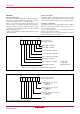
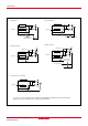
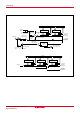
Fig. 15 Block diagram of ports (2)
(9) Ports P36, P37
Data bus
Port latch
Pull-up control
INT interrupt input
*
(7) Ports P20–P27
Analog input pin selection bit
A/D converter input
Data bus
Port latch
(8) Ports P30–P35
Data bus
Port latch
Pull-up control
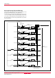
(6) Ports P14
CNTR
0
interrupt input
Direction register
Data bus
Port latch
Pulse output mode
Timer output
P3
7
/INT
0
input
level selection bit
(10) Ports P15, P16, P40, P41
Data bus
Port latch
Direction register
Direction register
Direction register
Direction register
: P10, P12, P13, P36, P37 input levels are switched to the CMOS/TTL level by the port P1P3 control register.
When the TTL level is selected, there is no hysteresis characteristics.
*