7534 Group REJ03B0099-0300 Rev.3.00 Oct 23, 2006 SINGLE-CHIP 8-BIT CMOS MICROCOMPUTER • DESCRIPTION The 7534 Group is the 8-bit microcomputer based on the 740 family core technology. The 7534 Group has a USB, 8-bit timers, and an A/D converter, and is useful for an input device for personal computer peripherals. FEATURES • • • • • • Basic machine-language instructions ....................................... 69 The minimum instruction execution time .......................... 0.
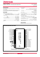
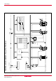
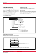
7534 Group 17 18 19 20 21 22 25 16 26 15 27 14 28 M37534M4-XXXGP 13 9 P34(LED4) P33(LED3) P32(LED2) P31(LED1) P30(LED0) VSS XOUT XIN P22/AN2 P23/AN3 P24/AN4 P25/AN5 VREF RESET CNVSS VCC 8 32 7 10 6 31 5 11 4 30 3 12 2 29 1 P07 P10/RXD/DP11/TXD/D+ P12/SCLK P13/SDATA P14/CNTR0 P20/AN0 P21/AN1 23 24 P06 P05 P04 P03 P02 P01 P00 USBVREFOUT PIN CONFIGURATION (TOP VIEW) Outline PLQP0032GB-A (32P6U-A) Fig. 2 Pin configuration of M37534M4-XXXGP Rev.3.
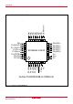
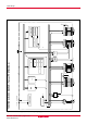
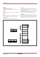
7534 Group PIN CONFIGURATION (TOP VIEW) 1 42 2 41 3 40 4 39 5 38 6 37 7 8 9 10 11 12 13 14 15 16 17 M37534RSS M37534M4-XXXSP M37534E8SP P14/CNTR0 P15 P16 P20/AN0 P21/AN1 NC P22/AN2 P23/AN3 P24/AN4 P25/AN5 P26/AN6 P27/AN7 P40 P41 VREF RESET CNVSS Vcc XIN XOUT VSS 36 35 34 33 32 31 30 29 28 27 26 18 25 19 24 20 23 21 22 P13/SDATA P12/SCLK P11/TXD/D+ P10/RXD/DP07 P06 P05 P04 P03 P02 P01 P00 USBVREFOUT P37/INT0 P36(LED6)/INT1 P35(LED5) P34(LED4) P33(LED3) P32(LED2) P31(LED1) P30(LED0)
Rev.3.00 Oct 23, 2006 REJ03B0099-0300 page 4 of 53 Fig.
Rev.3.00 Oct 23, 2006 REJ03B0099-0300 page 5 of 53 Fig.
Rev.3.00 Oct 23, 2006 REJ03B0099-0300 20 page 6 of 53 Fig.
534 Group PIN DESCRIPTION Table 1 Pin description Pin Name Function Function expect a port function •Apply voltage of 4.1 to 5.5 V (4.4 to 5.25 V at USB operating) to Vcc, and 0 V to Vss. Vcc, Vss Power source VREF Analog reference voltage •Reference voltage input pin for A/D converter USBVREFOUT USB reference voltage output •Output pin for pulling up a D- line with 1.5 kΩ external resistor CNVss CNVss •Chip operating mode control pin, which is always connected to Vss.
7534 Group GROUP EXPANSION Renesas expands the 7534 group as follow: Memory type Support for Mask ROM version, One Time PROM version, and Emulator MCU . Package PRSP0036GA-A ......................... 0.8 mm-pitch plastic molded SOP PLQP0032GB-A ........................ 0.8 mm-pitch plastic molded LQFP PRDP0042BA-A .................................... 42 pin plastic molded SDIP 42SIM ...................................... 42 pin shrink ceramic PIGGY BACK Memory size ROM/PROM size .........................
7534 Group FUNCTIONAL DESCRIPTION [CPU Mode Register] CPUM The CPU mode register contains the stack page selection bit. This register is allocated at address 003B16. Central Processing Unit (CPU) The 7534 Group uses the standard 740 family instruction set. Refer to the table of 740 family addressing modes and machine-language instructions or the 740 Family Software Manual for details on each instruction set. Machine-resident 740 family instructions are as follows: 1.
7534 Group Memory Special function register (SFR) area The SFR area in the zero page contains control registers such as I/O ports and timers. RAM RAM is used for data storage and for a stack area of subroutine calls and interrupts. ROM The first 128 bytes and the last 2 bytes of ROM are reserved for device testing and the rest is a user area for storing programs. Interrupt vector area The interrupt vector area contains reset and interrupt vectors.
7534 Group 000016 Port P0 (P0) 002016 USB interrupt control register (USBICON) 000116 Port P0 direction register (P0D) 002116 USB transmit data byte number set register 0 (EP0BYTE) 000216 Port P1 (P1) 002216 USB transmit data byte number set register 1 (EP1BYTE) 000316 Port P1 direction register (P1D) 002316 USBPID control register 0 (EP0PID) 000416 Port P2 (P2) 002416 USBPID control register 1 (EP1PID) 000516 Port P2 direction register (P2D) 002516 USB address register (USBA) 00061
7534 Group I/O Ports [Direction registers] PiD The I/O ports have direction registers which determine the input/output direction of each pin. Each bit in a direction register corresponds to one pin, and each pin can be set to be input or output. When “1” is set to the bit corresponding to a pin, this pin becomes an output port. When “0” is set to the bit, the pin becomes an input port. When data is read from a pin set to output, not the value of the pin itself but the value of port latch is read.
7534 Group Table 3 I/O port function table Pin Name Input/output P00–P07 P10/RxD/DP11/TxD/D+ I/O format Non-port function Related SFRs Diagram No.
7534 Group (2) Port P10 (1) Port P0 Serial I/O1 mode selection bit (b7) Serial I/O1 mode selection bit (b6) Receive enable bit Pull-up control Direction register Data bus Serial I/O1 mode selection bit (b7) Serial I/O1 mode selection bit (b6) Direction register Port latch Data bus Port latch P10,P12,P13 input level selection bit To key input interrupt generating circuit Serial I/O1 input * (3) Port P11 D- input P-channel output disable bit D- output Serial I/O1 mode selection bit (b7) Serial I/
7534 Group (7) Ports P20–P27 (6) Ports P14 Direction register Direction register Port latch Data bus Data bus Port latch Pulse output mode Timer output A/D converter input Analog input pin selection bit CNTR0 interrupt input (9) Ports P36, P37 (8) Ports P30–P35 Pull-up control Pull-up control Direction register Direction register Data bus Data bus Port latch Port latch P37/INT0 input level selection bit INT interrupt input * (10) Ports P15, P16, P40, P41 Direction register Data bus
7534 Group Interrupts Interrupts occur by 14 different sources : 4 external sources, 9 internal sources and 1 software source. Interrupt control All interrupts except the BRK instruction interrupt have an interrupt request bit and an interrupt enable bit, and they are controlled by the interrupt disable flag. When the interrupt enable bit and the interrupt request bit are set to “1” and the interrupt disable flag is set to “0”, an interrupt is accepted.
7534 Group Interrupt request bit Interrupt enable bit Interrupt disable flag I BRK instruction Reset Fig.
7534 Group Key Input Interrupt (Key-On Wake-Up) A key-on wake-up interrupt request is generated by applying “L” level to any pin of port P0 that has been set to input mode. In other words, it is generated when the AND of input level goes from “1” to “0”. An example of using a key input interrupt is shown in Figure 18, where an interrupt request is generated by pressing one of the keys provided as an active-low key matrix which uses ports P00 to P03 as input ports.
7534 Group Timers The 7534 Group has 3 timers: timer X, timer 1 and timer 2. The division ratio of every timer and prescaler is 1/(n+1) provided that the value of the timer latch or prescaler is n. All the timers are down count timers. When a timer reaches “0”, an underflow occurs at the next count pulse, and the corresponding timer latch is reloaded into the timer. When a timer underflows, the interrupt request bit corresponding to each timer is set to “1”.
7534 Group Data bus f(XIN)/16 f(XIN)/2 Prescaler X latch (8) Timer X count source selection bit Pulse width measurement mode CNTR0 active edge switch bit “0” P14/CNTR0 Prescaler X (8) Event counter mode Timer X latch (8) Timer mode pulse output mode Timer X (8) To timer X interrupt request bit Timer X count stop bit To CNTR0 interrupt request bit “1” CNTR0 active edge switch bit “1” Q Q “0” Toggle flip-flop R T Timer X latch write Pulse output mode Port P14 latch Port P14 direction register
7534 Group Serial Interface ●Serial I/O1 • Asynchronous serial I/O (UART) mode Serial I/O1 can be used as an asynchronous (UART) serial I/O. A dedicated timer (baud rate generator) is also provided for baud rate generation when serial I/O1 is in operation. Eight serial data transfer formats can be selected, and the transfer formats to be used by a transmitter and a receiver must be identical. Each of the transmit and receive shift registers has a buffer register (the same address on memory).
7534 Group [Serial I/O1 control register] SIO1CON The serial I/O1 control register consists of eight control bits for the serial I/O1 function. [Baud Rate Generator] BRG The baud rate generator determines the baud rate for serial transfer. The baud rate generator divides the frequency of the count source by 1/(n + 1), where n is the value written to the baud rate generator.
7534 Group USB status/UART status register functions as the USB status register (USBSTS).There is the USBVREFOUT pin for the USB reference voltage output, and a D-line with 1.5 kΩ external resistor can be pull up. USB mode block and USB transceiver block shown in figures 25 and 26. • Universal serial bus (USB) mode By setting bits 7 and 6 of the serial I/O1 control register (address 001A16) to “11”, the USB mode is selected. This mode conforms to Low-Speed USB2.0 specification.
7534 Group b7 b0 Transmit buffer register (TB: address 0018 16) After setting data to address 0018 16, a content of the transmit buffer register transfers to the transmit shift register automatically. CPU read: Disabled CPU write: Set/Clear Hardware read: Used Hardware write: Not used b7 b0 Receive buffer register (RB: address 0018 16) By reading data from address 0018 16, a content of the receive buffer register can be read out.
7534 Group b7 b0 USB data toggle synchronization register (TRSYNC: address 001D 16) Not used (return “1” when read) Sequence bit toggle flag 0: No toggle 1: Sequence toggle b7 CPU read: Enabled CPU write: Clear Hardware read: Not used Hardware write: Set b0 USB interrupt source discrimination register 1 (USBIR1: address 001E 16) Not used (return “1” when read) Endpoint determination flag 0: Endpoint 0 interrupt 1: Endpoint 1 interrupt b7 CPU read: Enabled CPU write: Disabled Hardware read: Not used H
7534 Group b7 b0 USB transmit data byte number set register 0 (EP0BYTE: address 002116) Set a number of data byte for transmitting with endpoint 0. CPU read: Enabled CPU write: Set/Clear Hardware read: Used Hardware write: Not used Not used (return “0” when read) b7 b0 USB transmit data byte number set register 1 (EP1BYTE: address 002216) Set a number of data byte for transmitting with endpoint 1.
7534 Group b7 b0 USB sequence bit initialization register (INISQ1: address 0026 16) A sequence bit of endpoint 1 is initialized.
7534 Group b7 b0 UART control register (UARTCON: address 001B 16) Character length selection bit 0: 8 bits 1: 7 bits Parity enable bit 0: Parity checking disabled 1: Parity checking enabled Parity selection bit 0: Even parity 1: Odd parity CPU read: Disabled CPU write: Set/Clear Hardware read: Used Hardware write: Not used Stop bit length selection bit 0: 1 stop bit 1: 2 stop bits P-channel output disable bit 0: CMOS output 1: N-channel open-drain output Not used (returns “1” when read) b7 b0 Serial
7534 Group Note on using USB mode Handling of SE0 signal in program (at receiving) 7534 group has the border line to detect as USB RESET or EOP (End of Packet) on the width of SE0 (Single Ended 0). A response apposite to a state of the device is expected. The name of the following short words which is used in table 5 shows as follow.
7534 Group ●Serial I/O2 b7 The serial I/O2 function can be used only for clock synchronous serial I/O. For clock synchronous serial I/O2 the transmitter and the receiver must use the same clock. When the internal clock is used, transfer is started by a write signal to the serial I/O2 register.
7534 Group Serial I/O2 operation By writing to the serial I/O2 register(address 003116) the serial I/O2 counter is set to “7”. After writing, the SDATA pin outputs data every time the transfer clock shifts from a high to a low level. And, as the transfer clock shifts from a low to a high, the SDATA pin reads data, and at the same time the contents of the serial I/O2 register are shifted by 1 bit.
7534 Group A/D Converter b7 The functional blocks of the A/D converter are described below. b0 A/D control register (ADCON : address 003416) [A/D conversion register] AD The A/D conversion register is a read-only register that stores the result of A/D conversion. Do not read out this register during an A/D conversion.
7534 Group Watchdog Timer The watchdog timer gives a means for returning to a reset status when the program fails to run on its normal loop due to a runaway. The watchdog timer consists of an 8-bit watchdog timer H and an 8bit watchdog timer L, being a 16-bit counter. Standard operation of watchdog timer The watchdog timer stops when the watchdog timer control register (address 003916) is not set after reset.
7534 Group Reset Circuit The microcomputer is put into a reset status by holding the RESET pin at the “L” level for 15 µs or more when the power source voltage is 4.1 to 5.5 V and XIN is in stable oscillation. After that, this reset status is released by returning the RESET pin to the “H” level. The program starts from the address having the contents of address FFFD16 as high-order address and the contents of address FFFC16 as low-order address. Note that the reset input voltage should be 0.
7534 Group Address Register contents (1) Port P0 direction register 000116 (2) Port P1 direction register 000316 (3) Port P2 direction register 000516 0016 (4) Port P3 direction register 000716 0016 (5) Port P4 direction register 000916 (6) Pull-up control register 001616 (7) USB/UART status register 001916 (8) Serial I/O1 control register 001A16 (9) UART control register 001B16 1 1 1 0 (10) USB data toggle synchronization register 001D16 0 1 1 (11) USB interrupt source discr
7534 Group Clock Generating Circuit An oscillation circuit can be formed by connecting a resonator between XIN and XOUT. Use the circuit constants in accordance with the resonator manufacturer's recommended values. No external resistor is needed between XIN and XOUT since a feed-back resistor exists on-chip. (An external feed-back resistor may be needed depending on conditions.
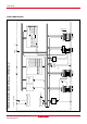
7534 Group XIN XOUT (Note 2) Rf Rd Clock division ratio selection bit Middle-speed, High-speed, double -speed mode 1/2 1/2 1/4 Timer 1 Prescaler 12 On-chip oscillator mode Clock division ratio selection bit Middle-speed mode Timing φ (Internal clock) High-speed mode Double-speed mode On-chip oscillator (Note 1) 1/8 On-chip oscillator mode S Q S STP instruction R Reset Interrupt disable flag l Interrupt request WIT instruction Q R page 37 of 53 S R STP instruction Note 1: On-chip o
7534 Group NOTES ON PROGRAMMING Processor Status Register The contents of the processor status register (PS) after reset are undefined except for the interrupt disable flag I which is “1”. After reset, initialize flags which affect program execution. In particular, it is essential to initialize the T flag and the D flag because of their effect on calculations.
7534 Group Note on A/D Converter SUSPEND Routine Configuration to CMOS input level for P10, P12, P13 input level. P1P3C xxxxx0xx2 Configuration to CMOS input level for P10, P12, P13 input level. P1P3C xxxxx1xx2 Configuration to TTL input level for P10, P12, P13 input level. STP Method to stabilize A/D Converter is described below. (a) A/D conversion accuracy could be affected for Bus Powered*1 USB devices, while the communicating.
7534 Group ROM PROGRAMMING METHOD The built-in PROM of the blank One Time PROM version can be read or programmed with a general-purpose PROM programmer using a special programming adapter. Set the address of PROM programmer in the user ROM area.
7534 Group ELECTRICAL CHARACTERISTICS Absolute Maximum Ratings Table 7 Absolute maximum ratings Parameter Symbol VCC Power source voltage VI Input voltage P00–P07, P10–P16, P20–P27, P30– P37, VREF, P40, P41 VI Input voltage RESET, XIN VI Input voltage CNVSS (Note 1) Conditions All voltages are based on VSS. Output transistors are cut off. Ratings Unit –0.3 to 7.0 V –0.3 to VCC + 0.3 V –0.3 to VCC + 0.3 V –0.3 to 13 V –0.3 to VCC + 0.
7534 Group Recommended Operating Conditions Table 8 Recommended operating conditions (VCC = 4.1 to 5.5 V, Ta = –20 to 85 °C, unless otherwise noted) Symbol Limits Parameter VCC Power source voltage VSS Power source voltage VREF Analog reference voltage VIH “H” input voltage P00–P07, P10–P16, P20–P27, P30–P37, P40, P41 VIH “H” input voltage (TTL input level selected) P10, P12, P13, P36, P37 VIH “H” input voltage RESET, XIN VIH “H” input voltage D+, D- f(XIN) = 6 MHz Min. Typ. Max.
7534 Group Electrical Characteristics Table 9 Electrical characteristics (1) (VCC = 4.1 to 5.5 V, VSS = 0 V, Ta = –20 to 85 °C, unless otherwise noted) Symbol VOH Parameter “H” output voltage P00–P07, P10–P16, P20–P27, P30–P37, P40, P41 (Note 1) Test conditions Limits Min. Typ. Max. Unit IOH = –5 mA VCC = 4.1 to 5.5 V VCC–1.5 V IOH = –1.0 mA VCC = 4.1 to 5.5 V VCC–1.0 V VOH “H” output voltage D+, D- VCC = 4.4 to 5.25 V Pull-down through 15kΩ ±5 % for D+, DPull-up through 1.
7534 Group Table 10 Electrical characteristics (2) (VCC = 4.1 to 5.5 V, VSS = 0 V, Ta = –20 to 85 °C, unless otherwise noted) Symbol Parameter Power source current ICC Limits Test conditions Min. Unit Typ. Max. 6 10 mA f(XIN) = 6 MHz, (in WIT state) Output transistors “off” 1.6 3.2 mA Increment when A/D conversion is executed f(XIN) = 6 MHz, VCC = 5 V 0.8 Double-speed mode, f(XIN) = 6 MHz, Output transistors “off” All oscillation stopped (in STP state) Output transistors “off” VCC = 4.
7534 Group Timing Requirements Table 12 Timing requirements (VCC = 4.1 to 5.5 V, VSS = 0 V, Ta = –20 to 85 °C, unless otherwise noted) Symbol Parameter Limits Min. Typ. Max.
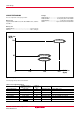
7534 Group tC(CNTR) tWL(CNTR) tWH(CNTR) CNTR0 0.8VCC 0.2VCC tWL(INT) tWH(INT) 0.8VCC INT0/INT1 0.2VCC tW(RESET) RESET 0.8VCC 0.2VCC tC(XIN) tWL(XIN) tWH(XIN) 0.8VCC XIN 0.2VCC tC(SCLK) tf SCLK tWL(SCLK) tr tWH(SCLK) 0.8VCC 0.2VCC tsu(SDATA-SCLK) th(SCLK-SDATA) 0.8VCC 0.2VCC SDATA(at receive) td(SCLK-SDATA) tv(SCLK-SDATA) SDATA(at transmit) tf D+, D- tr 0.1V0H Fig. 52 Timing chart Rev.3.00 Oct 23, 2006 REJ03B0099-0300 page 46 of 53 0.
7534 Group Description of improved USB function for 7534 Group Table 14 Description of improved USB function for 7534 Group Parameter No. 1 Response at Control transfer 7532/7536 Group Not deal with the host which performs the Control transfer in parallel to plural device. USB function can be used only at the condition of CL = 150 pF to 350 pF.
7534 Group Additionally, there are differences of SFR usage and functional definitions.
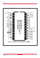
7534 Group Description supplement for use of USB function stably P27/AN7 VREF RESET CNVSS Vcc XIN XOUT VSS 1 36 2 35 3 34 4 33 5 6 7 8 9 10 11 12 13 14 15 M37534M4-XXXFP M37534E8FP P12/SCLK P13/SDATA P14/CNTR0 P20/AN0 P21/AN1 P22/AN2 P23/AN3 P24/AN4 P25/AN5 P26/AN6 32 31 30 29 28 27 26 25 24 23 22 16 21 17 20 18 19 P11/TXD/D+ P10/RXD/DP07 P06 P05 P04 P03 P02 P01 P00 USBVREFOUT P37/INT0 P35(LED5) P34(LED4) P33(LED3) P32(LED2) P31(LED1) P30(LED0) 1.
7534 Group ➁ Connect a capacitor to a device as close as possible. For the capacitor, a ceramic capacitor or an electrolytic capacitor of 0.22 µF is recommended.
7534 Group 1 42 2 41 3 40 4 39 5 38 6 37 7 8 9 10 11 12 13 14 15 16 17 M37534E8SP M37534M4-XXXSP M37534RSS P14/CNTR0 P15 P16 P20/AN0 P21/AN1 NC P22/AN2 P23/AN3 P24/AN4 P25/AN5 P26/AN6 P27/AN7 P40 P41 VREF RESET CNVSS Vcc XIN XOUT VSS 36 35 34 33 32 31 30 29 28 27 26 18 25 19 24 20 23 21 22 P13/SDATA P12/SCLK P11/TXD/D+ P10/RXD/DP07 P06 P05 P04 P03 P02 P01 P00 USBVREFOUT P37/INT0 P36(LED6)/INT1 P35(LED5) P34(LED4) P33(LED3) P32(LED2) P31(LED1) P30(LED0) Outline PRDP0042BA-A ➀ Conne
7534 Group PACKAGE OUTLINE PLQP0032GB-A JEITA Package Code P-LQFP32-7x7-0.80 RENESAS Code PLQP0032GB-A Previous Code 32P6U-A MASS[Typ.] 0.2g HD *1 D 24 17 NOTE) 1. * *2" * INCLUDE TRIM OFFSET. 16 25 bp c HE *2 E b1 Reference Dimension in Millimeters Symbol D E A HD 32 9 ZE Terminal cross section E 1 Min Nom Max 6.9 7.0 7.1 6.9 7.0 7.1 8.8 8.8 9.0 9.2 8 ZD Index mark A1 p c A1 A A2 F L b1 c c1 L1 y *3 e e x y ZD ZE L L1 Detail F bp 0.1 0.2 0.42 0.35 0.09 0.145 0.
7534 Group PRDP0042BA-A RENESAS Code PRDP0042BA-A Previous Code 42P4B MASS[Typ.] 4.1g 22 1 21 *1 E 42 e1 JEITA Package Code P-SDIP42-13x36.72-1.78 *2" 2. INCLUDE TRIM OFFSET. D A 2 *2 c NOTE) 1. L A1 Reference Symbol SEATING PLANE e Rev.3.00 Oct 23, 2006 REJ03B0099-0300 *3 b3 page 53 of 53 bp *3 b2 Dimension in Millimeters Min Nom Max e1 14.94 15.24 15.54 D 36.5 36.7 36.9 E 12.85 13.0 13.15 A 5.5 A1 0.51 A2 3.8 bp 0.35 0.45 0.55 b2 0.63 0.73 1.03 b3 0.9 1.0 1.3 c 0.22 0.27 0.
REVISION HISTORY Rev. 7534 Group DATA SHEET Date Description Summary Page 1.00 Jan. 18, 2000 – First edition issued 1.10 Jun. 14, 2000 2 5 8 34 43 44 48 49 50 51 package type revised; 32P6B-A → 32P6U-A package type revised; 32P6B-A → 32P6U-A package type revised; 32P6B-A → 32P6U-A ____________ Description revised; RESET “L” pulse width 2 µs → 15 µs Table 11 revised; Absolute accuracy (excluding quantization error) → Linearity error ____________ Table 12 revised; tw(RESET): 2 → 15 Fig.
REVISION HISTORY Rev. 7534 Group DATA SHEET Date Description Summary Page 3.00 Oct.
Sales Strategic Planning Div. Nippon Bldg., 2-6-2, Ohte-machi, Chiyoda-ku, Tokyo 100-0004, Japan Notes: 1. This document is provided for reference purposes only so that Renesas customers may select the appropriate Renesas products for their use.