M37221M4H/M6H/M8H/MAH–XXXSP/FP M37221EASP/FP SINGLE-CHIP 8-BIT CMOS MICROCOMPUTER for VOLTAGE SYNTHESIZER with ON-SCREEN DISPLAY CONTROLLER 1. DESCRIPTION The M37221M4H/M6H/M8H/MAH-XXXSP/FP are single-chip microcomputers designed with CMOS silicon gate technology. They have a OSD, I2C-BUS interface, and PWM, making them perfect for TV channel selection system. The M37221EASP/FP have a built-in PROM that can be written electrically. ●OSD function Display characters ....................................
M37221M4H/M6H/M8H/MAH–XXXSP/FP M37221EASP/FP TABLE OF CONTENTS 1. DESCRIPTION ............................................................... 1 2. FEATURES .................................................................... 1 3. APPLICATION ................................................................ 1 4. PIN CONFIGURATION .................................................. 3 5. FUNCTIONAL BLOCK DIAGRAM ................................. 5 6. PERFORMANCE OVERVIEW .......................................
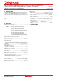
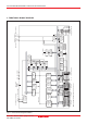
M37221M4H/M6H/M8H/MAH–XXXSP/FP M37221EASP/FP 4.
M37221M4H/M6H/M8H/MAH–XXXSP/FP M37221EASP/FP 1 42 P52/R VSYNC 2 41 P00/PWM0 P01/PWM1 P02/PWM2 3 40 P53/G P54/B 4 39 P55/OUT1 5 38 P03/PWM3 P04/PWM4 P05/PWM5 P06/INT2/A-D4 P07/INT1 6 37 P20/SCLK P21/SOUT 7 36 P22/SIN 8 35 10 33 P10/OUT2 P11/SCL1 P12/SCL2 P23/TIM3 11 32 P13/SDA1 P24/TIM2 12 31 P25 13 P14/SDA2 P15/A-D1/INT3 P26 14 P27 15 28 D-A 16 27 P16/A-D2 P17/A-D3 P30/A-D5/DA1 P32 17 26 P31/A-D6/DA2 CNVSS XIN XOUT VSS 18 25 19 24 20 23 RESET OSC1/P3
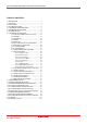
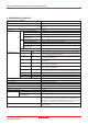
I/O port P1 I/O port P0 I/O port P2 15 14 13 12 11 36 37 38 Notes Only M37221EASP/FP has D-A converter.
M37221M4H/M6H/M8H/MAH–XXXSP/FP M37221EASP/FP 6. PERFORMANCE OVERVIEW Table 6.1 Performance Overview Parameter Functions Number of basic instructions 71 Number of basic instructions 0.
M37221M4H/M6H/M8H/MAH–XXXSP/FP M37221EASP/FP Table 6.2 Performance Overview (continued) Parameter OSD display function Number of display characters Dot structure 12 ✕ 16 dots Kinds of characters 256 kinds Kinds of character sizes 3 kinds Character font coloring 1 screen: 8 kinds (per character unit) Display position Horizontal: 64 levels, Vertical: 128 levels Power source voltage Power dissipation 5 V ± 10 % OSD ON 165 mW typ.
M37221M4H/M6H/M8H/MAH–XXXSP/FP M37221EASP/FP 7. PIN DESCRIPTION Table 7.1 Pin Description Pin Name Input/ Output Name VCC, VSS. Power source CNVSS CNVSS RESET Reset input Input To enter the reset state, the reset input pin must be kept at a “L” for 2 µs or more (under normal VCC conditions). If more time is needed for the quartz-crystal oscillator to stabilize, this “L” condition should be maintained for the required time.
M37221M4H/M6H/M8H/MAH–XXXSP/FP M37221EASP/FP Table 7.2 Pin Description (continued) Output port P5 Output Ports P5 2 –P5 5 are a 4-bit output port. The output structure is CMOS output. OSD output Output Pins P52–P55 are also used as OSD output pins R, G, B, OUT1 respectively. The output structure is CMOS output. HSYNC HSYNC input Input This is a horizontal synchronizing signal input for OSD. VSYNC VSYNC input Input This is a vertical synchronizing signal input for OSD.
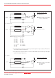
M37221M4H/M6H/M8H/MAH–XXXSP/FP M37221EASP/FP Ports P00–P05, P32 N-channel open drain output Direction register Ports P00–P05, P32 Port latch Data bus Note: Each port is also used as follows: P00–P05 : PWM0–PWM5 Ports P1, P2, P30, P31 Direction register CMOS output Data bus Ports P1, P2, P30, P31 Port latch Notes 1: Each port is also used as follows: P10 : OUT2 P20 : SCLK P11 : SCL1 P21 : SOUT P12 : SCL2 P22 : SIN P13 : SDA1 P23 : TIM3 P14 : SDA2 P24 : TIM2 P15 : A-D1/INT3 P30 : A-D5/D
M37221M4H/M6H/M8H/MAH–XXXSP/FP M37221EASP/FP HSYNC, VSYNC D-A, R, G, B, OUT1, OUT2 Schmidt input HSYNC, VSYNC Internal circuit Internal circuit CMOS output D-A, R, G, B, OUT1, OUT2 Note: Each pin is also used as below: R : P52 G : P53 B : P54 OUT1 : P55 OUT2 : P10 Fig. 7.2 I/O pin block diagram (2) Rev.1.
M37221M4H/M6H/M8H/MAH–XXXSP/FP M37221EASP/FP 8. FUNCTION BLOCK DESCRIPTION 8.1 CENTRAL PROCESSING UNIT (CPU) 8.1.1 CPU Mode Register This microcomputer uses the standard 740 Family instruction set. Refer to the table of 740 Family addressing modes and machine instructions or the SERIES 740 User’s Manual for details on the instruction set. Availability of 740 Family instructions is as follows: The FST and SLW instructions cannot be used. The MUL, DIV, WIT and STP instructions can be used.
M37221M4H/M6H/M8H/MAH–XXXSP/FP M37221EASP/FP 8.2 MEMORY 8.2.1 Special Function Register (SFR) Area The special function register (SFR) area in the zero page includes control registers such as I/O ports and timers. 8.2.2 RAM RAM is used for data storage and for stack area of subroutine calls and interrupts. 8.2.3 ROM ROM is used for storing user programs as well as the interrupt vector area. 8.2.4 OSD RAM 8.2.6 Interrupt Vector Area The interrupt vector area contains reset and interrupt vectors. 8.2.
M37221M4H/M6H/M8H/MAH–XXXSP/FP M37221EASP/FP ■ M37221M8H/MAH-XXXSP/FP, M37221EASP/FP 000016 1000016 Zero page OSD ROM (8K bytes) 00C016 SFR area 00FF16 M37221MAHXXXSP/FP, M37221EASP/FP RAM (704 bytes) M37221M8HXXXSP/FP RAM (576 bytes) 11FFF16 01FF16 021716 021B16 Not used 2 page register Not used 02C016 02E016 02FF16 030016 033F16 03BF16 ROM correction function Vector 1: address 02C016 Vector 2: address 02E016 Not used OSD RAM (96 bytes) (See note) M37221MAHXXXSP/FP, M37221EASP/FP RAM (40K bytes
M37221M4H/M6H/M8H/MAH–XXXSP/FP M37221EASP/FP ■ SFR area (addresses C016 to DF16) : State immediately after reset> 0 : “0” immediately after reset Function bit Name : 1 : “1” immediately after reset : No function bit 0 : Fix to this bit to “0” (do not write to “1”) ? : Indeterminate immediately after reset 1 : Fix to this bit to “1” (do not write to “0”) Address C016 C116 C216 C316 C416 C516 C616 C716 C816 C916 CA16 CB16 CC16 CD16 CE16 CF16 D016 D116 D216 D316 D416 D516 D616 D716 D8
M37221M4H/M6H/M8H/MAH–XXXSP/FP M37221EASP/FP ■ SFR area (addresses E016 to FF16) : 0 : “0” immediately after reset Function bit Name : 1 : “1” immediately after reset : No function bit ? 0 : Fix to this bit to “0” (do not write to “1”) 1 : Fix to this bit to “1” (do not write to “0”) Address E016 E116 E216 E316 E416 E516 E616 E716 E816 E916 EA16 EB16 EC16 ED16 EE16 EF16 F016 F116 F216 F316 F416 F516 F616 F716 F816 F916 FA16 FB16 FC16 FD16 FE16 FF16
M37221M4H/M6H/M8H/MAH–XXXSP/FP M37221EASP/FP ■ 2 page register area (addresses 21716 to 21B16) : State immediately after reset> 0 : “0” immediately after reset Function bit Name : 1 : “1” immediately after reset : No function bit ? : Indeterminate immediately after reset 0 : Fix to this bit to “0” (do not write to “1”) 1 : Fix to this bit to “1” (do not write to “0”) Address 21716 21816 21916 21A16 21B16 Register Bit allocation b7 State immediately after reset b 0 b7 ROM correc
M37221M4H/M6H/M8H/MAH–XXXSP/FP M37221EASP/FP : Name 0 : “0” immediately after reset Function bit : 1 : “1” immediately after reset : No function bit ? : Indeterminate immediately after reset 0 : Fix to this bit to “0” (do not write to “1”) 1 : Fix to this bit to “1” (do not write to “0”) Register Bit allocation State immediately after reset b0 b7 b7 Processor status register (PS) Program counter (PCH) N V T B D I Z C Program counter (PCL)
M37221M4H/M6H/M8H/MAH–XXXSP/FP M37221EASP/FP 8.3 INTERRUPTS Interrupts can be caused by 14 different sources comprising 4 external, 8 internal, 1 software, and 1 reset interrupts. Interrupts are vectored interrupts with priorities as shown in Table 8.3.1. Reset is also included in the table as its operation is similar to an interrupt. When an interrupt is accepted, ① The contents of the program counter and processor status register are automatically stored into the stack.
M37221M4H/M6H/M8H/MAH–XXXSP/FP M37221EASP/FP (4) Serial I/O interrupt This is an interrupt request from the clock synchronous serial I/O function. (5) f(XIN)/4096 interrupt The f (XIN)/4096 interrupt occurs regularly with a f(XIN)/4096 period. Set bit 0 of PWM output control register 1 to “0.” (6) Multi-master I2C-BUS interface interrupt Interrupt request bit Interrupt enable bit Interrupt disable flag I This is an interrupt request related to the multi-master I2C-BUS interface.
M37221M4H/M6H/M8H/MAH–XXXSP/FP M37221EASP/FP Interrupt Request Register 1 b7 b6 b5 b4 b3 b2 b1 b0 Interrupt request register 1 (IREQ1) [Address 00FC16] B Name 0 Timer 1 interrupt request bit (TM1R) Functions After reset 0 0 : No interrupt request issued 1 : Interrupt request issued Timer 2 interrupt 0 0 : No interrupt request issued request bit (TM2R) 1 : Interrupt request issued 0 Timer 3 interrupt 0 : No interrupt request issued request bit (TM3R) 1 : Interrupt request issued 0 Timer 4 interrupt 0 : No
M37221M4H/M6H/M8H/MAH–XXXSP/FP M37221EASP/FP Interrupt Control Register 1 b7 b6 b5 b4 b3 b2 b1 b0 Interrupt control register 1 (ICON1) [Address 00FE16] B Name Functions After reset R W 0 Timer 1 interrupt enable bit (TM1E) 1 Timer 2 interrupt enable bit (TM2E) 0 : Interrupt disabled 1 : Interrupt enabled 0 : Interrupt disabled 1 : Interrupt enabled 0 R W 0 R W 2 Timer 3 interrupt enable bit (TM3E) 0 : Interrupt disabled 1 : Interrupt enabled 0 R W 3 Timer 4 interrupt enable bit (TM4E) 4 OSD i
M37221M4H/M6H/M8H/MAH–XXXSP/FP M37221EASP/FP Interrupt Input Polarity Register b7 b6 b5 b4 b3 b2 b1 b0 0 0 0 Interrupt input polarity register(RE) [Address 00F916 ] B Name Functions 0 Nothing is assigned. This bit is a write disable bit. After reset R W 0 R — 0 R W When this bit is read out, the value is “0.” 1,2 Fix These bits to “0.
M37221M4H/M6H/M8H/MAH–XXXSP/FP M37221EASP/FP 8.4 TIMERS This microcomputer has 4 timers: timers 1 to 4. All timers are 8-bit timers with the 8-bit timer latch. The timer block diagram is shown in Figure 8.4.3. All of the timers count down and their divide ratio is 1/(n+1), where n is the value of timer latch. By writing a count value to the corresponding timer latch (addresses 00F016 to 00F316 : timers 1 to 4), the value is also set to a timer, simultaneously. The count value is decremented by 1.
M37221M4H/M6H/M8H/MAH–XXXSP/FP M37221EASP/FP Timer 12 Mode Register b7 b6 b5 b4 b3 b2 b1 b0 0 Timer mode register (T12M) [Address 00F416] Name B Functions After reset R W 0 Timer 1 count source 0: f(XIN)/16 selection bit 1 (T12M0) 1: f(XIN)/4096 0 R W 1 Timer 2 count source selection bit (T12M1) 0: Interrupt clock source 1: External clock from TIM2 pin 0 R W 2 Timer 1 count stop bit (T12M2) 0: Count start 1: Count stop 0 R W 3 Timer 2 count stop bit (T12M3) 0: Count start 1: Count stop
M37221M4H/M6H/M8H/MAH–XXXSP/FP M37221EASP/FP Data bus 8 Timer 1 latch (8) 1/4096 8 XIN 1/2 1/8 Timer 1 interrupt request Timer 1 (8) T12M0 T12M2 8 T12M4 8 Timer 2 latch (8) 8 TIM2 Timer 2 interrupt request Timer 2 (8) T12M1 T12M3 8 HSYNC 8 FF16 T34M5 TIM3 Reset STP instruction Timer 3 latch (8) 8 Timer 3 interrupt request Timer 3 (8) T34M0 T34M2 8 8 Selection gate : Connected to black colored side at reset 0716 T34M1 Timer 4 latch (8) T12M : Timer 12 mode register T34M : Timer 34 m
M37221M4H/M6H/M8H/MAH–XXXSP/FP M37221EASP/FP 8.5 SERIAL I/O This microcomputer has a built-in serial I/O which can either transmit or receive 8-bit data serially in the clock synchronous mode. The serial I/O block diagram is shown in Figure 8.5.1. The synchronous clock I/O pin (SCLK), data output pin (SOUT), and data input pin (SIN) also functions as port P2.
M37221M4H/M6H/M8H/MAH–XXXSP/FP M37221EASP/FP Internal clock : The serial I/O counter is set to “7” during the write cycle into the serial I/O register (address 00DD16), and the transfer clock goes HIGH forcibly. At each falling edge of the transfer clock after the write cycle, serial data is output from the SOUT pin. Transfer direction can be selected by bit 5 of the serial I/O mode register.
M37221M4H/M6H/M8H/MAH–XXXSP/FP M37221EASP/FP Serial I/O Mode Register b7 b6 b5 b4 b3 b2 b1 b0 0 Serial I/O mode register (SM) [Address 00DC16] B Name 0, 1 Internal synchronous clock selection bits (SM0, SM1) Functions b1 b0 0 0: f(XIN)/4 0 1: f(XIN)/16 1 0: f(XIN)/32 1 1: f(XIN)/64 2 Synchronous clock selection bit (SM2) 0: External clock 1: Internal clock 0 R W 3 Serial I/O port selection bit (SM3) 0: P20, P21 1: SCLK, SOUT 0 R W 0 R W 4 Fix this bit to “0.
M37221M4H/M6H/M8H/MAH–XXXSP/FP M37221EASP/FP 8.5.1 Serial I/O Common Transmission/Reception mode By writing “1” to bit 6 of the serial I/O mode register, signals SIN and SOUT are switched internally to be able to transmit or receive the serial data. Figure 8.5.4 shows signals on serial I/O common transmission/reception mode. Note: When receiving the serial data after writing “FF16” to the serial I/O register.
M37221M4H/M6H/M8H/MAH–XXXSP/FP M37221EASP/FP 8.6 MULTI-MASTER I2C-BUS INTERFACE Table 8.6.1 Multi-master I2C-BUS Interface Functions The multi-master I2C-BUS interface is a serial communications circuit, conforming to the Philips I2C-BUS data transfer format. This interface, offering both arbitration lost detection and a synchronous functions, is useful for the multi-master serial communications. Figure 8.6.1 shows a block diagram of the multi-master I2C-BUS interface and Table 8.6.
M37221M4H/M6H/M8H/MAH–XXXSP/FP M37221EASP/FP 8.6.1 I2C Data Shift Register The I2C data shift register (S0 : address 00D716) is an 8-bit shift register to store receive data and write transmit data. When transmit data is written into this register, it is transferred to the outside from bit 7 in synchronization with the SCL clock, and each time one-bit data is output, the data of this register are shifted one bit to the left.
M37221M4H/M6H/M8H/MAH–XXXSP/FP M37221EASP/FP 8.6.2 I2C Address Register The I2C address register (address 00D816) consists of a 7-bit slave address and a read/write bit. In the addressing mode, the slave address written in this register is compared with the address data to be received immediately after the START condition are detected. (1) Bit 0: read/write bit (RBW) Not used when comparing addresses, in the 7-bit addressing mode.
M37221M4H/M6H/M8H/MAH–XXXSP/FP M37221EASP/FP 8.6.3 I2C Clock Control Register (4) Bit 7: ACK clock bit (ACK) The I2C clock control register (address 00DB16) is used to set ACK control, SCL mode and SCL frequency. This bit specifies a mode of acknowledgment which is an acknowledgment response of data transmission. When this bit is set to “0,” the no ACK clock mode is set. In this case, no ACK clock occurs after data transmission.
M37221M4H/M6H/M8H/MAH–XXXSP/FP M37221EASP/FP 8.6.4 I2C Control Register (3) Bit 4: data format selection bit (ALS) The I2C control register (address 00DA16) controls the data communication format. This bit decides whether or not to recognize slave addresses. When this bit is set to “0,” the addressing format is selected, so that address data is recognized. When a match is found between a slave address and address data as a result of comparison or when a general call (refer to “8.6.
M37221M4H/M6H/M8H/MAH–XXXSP/FP M37221EASP/FP I2C Control Register b7 b6 b5 b4 b3 b2 b1 b0 I2C control register (S1D) [Address 00DA16] B Name After reset R W 0 to 2 Bit counter (Number of transmit/recieve bits) (BC0 to BC2) b2 0 0 0 0 1 1 1 1 b0 0: 8 1: 7 0: 6 1: 5 0: 4 1: 3 0: 2 1: 1 0 R W 3 I2C-BUS interface use enable bit (ESO) 0: Disabled 1: Enabled 0 R W 4 Data format selection bit(ALS) 0: Addressing format 1: Free data format 0 R W 5 Addressing format selection bit (10BIT SAD) 0:
M37221M4H/M6H/M8H/MAH–XXXSP/FP M37221EASP/FP 8.6.5 I2C Status Register The I2C status register (address 00D916) controls the I2C-BUS interface status. The low-order 4 bits are read-only bits and the highorder 4 bits can be read out and written to. (1) Bit 0: last receive bit (LRB) This bit stores the last bit value of received data and can also be used for ACK receive confirmation. If ACK is returned when an ACK clock occurs, the LRB bit is set to “0.” If ACK is not returned, this bit is set to “1.
M37221M4H/M6H/M8H/MAH–XXXSP/FP M37221EASP/FP (8) Bit 7: Communication mode specification bit (master/slave specification bit: MST) This bit is used for master/slave specification in data communications. When this bit is “0,” the slave is specified, so that a START condition and a STOP condition generated by the master are received, and data communication is performed in synchronization with the clock generated by the master.
M37221M4H/M6H/M8H/MAH–XXXSP/FP M37221EASP/FP 8.6.6 START Condition Generation Method When the ESO bit of the I2C control register (address 00DA16) is “1,” execute a write instruction to the I2C status register (address 00D916) to set the MST, TRX and BB bits to “1.” A START condition will then be generated. After that, the bit counter becomes “0002” and an SCL is output for 1 byte .
M37221M4H/M6H/M8H/MAH–XXXSP/FP M37221EASP/FP 8.6.8 START/STOP Condition Detect Conditions 8.6.9 Address Data Communication The START/STOP condition detect conditions are shown in Figure 8.6.11 and Table 8.6.3. Only when the 3 conditions of Table 8.6.3 are satisfied, a START/STOP condition can be detected. There are two address data communication formats, namely, 7-bit addressing format and 10-bit addressing format. The respective address communication formats are described below.
M37221M4H/M6H/M8H/MAH–XXXSP/FP M37221EASP/FP 8.6.10 Example of Master Transmission 8.6.11 Example of Slave Reception An example of master transmission in the standard clock mode, at the SCL frequency of 100 kHz with the ACK return mode enable, is shown below. ➀ Set a slave address in the high-order 7 bits of the I2C address register (address 00D816) and “0” in the RBW bit. ➁ Set the ACK return mode and SCL = 100 kHz by setting “8516” in the I2C clock control register (address 00DB16).
M37221M4H/M6H/M8H/MAH–XXXSP/FP M37221EASP/FP S Slave address R/W A Data A Data A/A P A P Data A 7 bits “ 0” 1 to 8 bits 1 to 8 bits (1) A master-transmitter transmits data to a slave-receiver S Slave address R/W A Data A Data 7 bits “ 1” 1 to 8 bits 1 to 8 bits (2) A master-receiver receives data from a slave-transmitter S Slave address R/W 1st 7 bits A Slave address 2nd byte A Data A/A P 1 to 8 bits 7 bits “ 0” 8 bits 1 to 8 bits (3) A master-transmitter transmits data to a sla
M37221M4H/M6H/M8H/MAH–XXXSP/FP M37221EASP/FP (3) RESTART condition generation procedure (4) STOP condition generation procedure ➀Procedure example (The necessary conditions for the procedure are described in ➁ to ➅ below.) Execute the following procedure when the PIN bit is “0.” ➀Procedure example (The necessary conditions for the procedure are described in ➁ to ➃ below.
M37221M4H/M6H/M8H/MAH–XXXSP/FP M37221EASP/FP 8.7 PWM OUTPUT FUNCTION 8.7.4 Operating of 14-bit PWM This microcomputer is equipped with two 14-bit PWM (DA) and six 8-bit PWMs (PWM0–PWM5). DA1 and DA2 have a 14-bit resolution with the minimum resolution bit width of 0.25 µs and a repeat period of 4096 µs (for f(XIN) = 8 MHz). PWM0–PWM7 have the same circuit structure and an 8-bit resolution with minimum resolution bit width of 4 µs and repeat period of 1024 µs (for f(XIN) = 8 MHz). Figure 8.7.
M37221M4H/M6H/M8H/MAH–XXXSP/FP M37221EASP/FP Fig. 8.7.1 PWM Block Diagram Rev.1.
Rev.1.00 Oct 01, 2002 REJ03B0134-0100Z Fig. 8.7.
M37221M4H/M6H/M8H/MAH–XXXSP/FP M37221EASP/FP Set “2816” to DA-L register. Set “2C16” to DA-H register. b7 b6 b5 b4 b3 b2 b1 b0 b7 b6 b5 b4 b3 b2 b1 b0 [DA-H 0 0 1 0 1 1 0 0 DH register] [DA-L register] b13 0 b6 b5 0 1 0 1 1 0 0 These bits decide HIGH level area of fundamental waveform. HIGH level area of fundamental waveform = Minimum resolution bit width 0.
M37221M4H/M6H/M8H/MAH–XXXSP/FP M37221EASP/FP PWM Output Control Register 1 b7 b6 b5 b4 b3 b2 b1 b0 PWM output control register 1 (PW) [Address 00D516] B Name Functions 0 DA, PWM count source 0 : Count source supply 1 : Count source stop selection bit (PW0) 0 : DA output 1 DA/PN4 selection bit 1 : PN4 output (PW1) After reset R W R W 0 0 R W 2 P00/PWM0 output selection bit (PW2) 0: P00 output 1: PWM0 output 0 R W 3 P01/PWM1 output selection bit (PW3) 0: P01 output 1: PWM1 output 0 R W 4 P02/PWM2
M37221M4H/M6H/M8H/MAH–XXXSP/FP M37221EASP/FP 8.8 A-D COMPARATOR A-D comparator consists of a 6-bit D-A converter and a comparator. The A-D comparator block diagram is shown in Figure 8.8.1. The reference voltage “Vref” for D-A conversion is set by bits 0 to 5 of the A-D control register 2 (address 00EF16). The comparison result of the analog input voltage and the reference voltage “Vref” is stored in bit 4 of the A-D control register 1 (address 00EE16).
M37221M4H/M6H/M8H/MAH–XXXSP/FP M37221EASP/FP A-D Control Register 1 b7 b6 b5 b4 b3 b2 b1 b0 A-D control register 1 (AD1) [Address 00EE16] B Name Functions 0 to 2 Analog input pin selection bits (ADM0 to ADM2) 3 This bit is a write disable bit. When this bit is read out, the value is “0.” 4 Storage bit of comparison result (ADM4) 5 to 7 Nothing is assigned. This bits are write disable bits. When these bits are read out, the values are “0.
M37221M4H/M6H/M8H/MAH–XXXSP/FP M37221EASP/FP 8.9 D-A CONVERTER This microcomputer has 2 D-A converters with 6-bit resolution. D-A converter block diagram is shown in Figure 8.9.1. D-A conversion is performed by setting the value in the DA conversion register. The result of D-A conversion is output from the DA pin by setting “1” to the DA output enable bit of the port P3 output mode control register (bits 2 and 3 at address 00CD16).
M37221M4H/M6H/M8H/MAH–XXXSP/FP M37221EASP/FP P3 output mode control register b7 b6 b5 b4 b3 b2 b1 b0 P3 output mode control register(P3S) [Address 00CD16] B 0 Name After reset R W Functions P30 output form selection bit (P30S) 0: CMOS output 1: N-channel open-drain output 0 R W 1 P31 output form selection bit (P31S) 0: CMOS output 1: N-channel open-drain output 0 R W 2 DA1 output enable bit (DA1S) 0: P30 input/output 1: DA1 output 0 R W 3 DA2 output enable bit (DA2S) 0: P31 input/output
M37221M4H/M6H/M8H/MAH–XXXSP/FP M37221EASP/FP 8.10 ROM CORRECTION FUNCTION This can correct program data in the ROM. Up to 2 addresses can be corrected ; a program for correction is stored in the ROM correction memory in the RAM as the top address. There are 2 vectors for ROM correction : Vector 1 : address 02C016 Vector 2 : address 02E016 Set the address of the ROM data to be corrected into the ROM correction address register.
M37221M4H/M6H/M8H/MAH–XXXSP/FP M37221EASP/FP 8.11 OSD FUNCTIONS Table 8.11.1 outlines the OSD functions. This microcomputer incorporates an OSD control circuit of 24 characters ✕ 2 lines. OSD is controlled by the CRT control register. Up to 256 kinds of characters can be displayed. The colors can be specified for each character and up to 4 kinds of colors can be displayed on one screen. A combination of up to 8 colors can be obtained by using each output signal (R, G, and B).
M37221M4H/M6H/M8H/MAH–XXXSP/FP M37221EASP/FP The OSD circuit has an extended display mode. This mode allows multiple lines (3 lines or more) to be displayed on the screen by interrupting the display each time one line is displayed and rewriting data in the block for which display has been terminated by software. Figure 8.11.1 shows the configuration of an OSD character. Figure 8.11.2 shows the block diagram of the OSD circuit. Figure 8.11.3 shows OSD control register. 12 dots 16 dots Fig. 8.11.
M37221M4H/M6H/M8H/MAH–XXXSP/FP M37221EASP/FP Clock for OSD OSC1 OSC2 HSYNC VSYNC Display oscillation circuit Control registers for OSD OSD Control circuit Horizontal position register Vertical position register Character size register Color register OSD control register OSD port control register OSD clock selection register (address 00E016) (addresses 00E116, 00E216) (addresses 00E416) (addresses 00E616 to 00E916) (address 00EA16 ) (address 00EC16) (address 00ED16) OSD RAM 10 bits ✕ 24 characters ✕ 2
M37221M4H/M6H/M8H/MAH–XXXSP/FP M37221EASP/FP OSD Control Register b7 b6 b5 b4 b3 b2 b1 b0 OSD control register (CC) [Address 00EA 16] B Functions Name After reset R W 0 R W 0 All-blocks display control bit (CC0) (See note) 0 : All-blocks display off 1 : All-blocks display on 1 Block 1 display control bit (CC1) 0 : Block 1 display off 1 : Block 1 display on 0 R W 2 Block 2 display control bit (CC2) 0 : Block 2 display off 1 : Block 2 display on 0 R W 3 to 6 Nothing is assigned.
M37221M4H/M6H/M8H/MAH–XXXSP/FP M37221EASP/FP 8.11.1 Display Position The display positions of characters are specified in units called “blocks.” There are 2 blocks : blocks 1 and 2. Up to 24 characters can be displayed in each block (refer to “8.11.3 Memory for OSD”). The display position of each block can be set in both horizontal and vertical directions by software.
M37221M4H/M6H/M8H/MAH–XXXSP/FP M37221EASP/FP The vertical display start position is determined by counting the horizontal sync signal (HSYNC). At this time, when VSYNC and HSYNC are positive polarity (negative polarity), the count starts at the rising edge (falling edge) of HSYNC signal after the fixed cycle of the rising edge (falling edge) of VSYNC signal.
M37221M4H/M6H/M8H/MAH–XXXSP/FP M37221EASP/FP The vertical display start position for each block can be set in 512 steps (where each step is 1TH (TH: HSYNC cycle)) as values “0016” to “7F16” in vertical position register i (i = 1 and 2) (addresses 00E116 and 00E216) The vertical position register i is shown in Figure 8.11.6.
M37221M4H/M6H/M8H/MAH–XXXSP/FP M37221EASP/FP The horizontal display start position is common to all blocks, and can be set in 64 steps (where 1 step is 4TC, TC being the OSD oscillation cycle) as values “0016” to “3F16” in bits 0 to 5 of the horizontal position register (address 00D116). The horizontal position register is shown in Figure 8.11.7.
M37221M4H/M6H/M8H/MAH–XXXSP/FP M37221EASP/FP 8.11.2 Character Size The size of characters to be displayed can be from 3 sizes for each block. Use the character size register (address 00E416) to set a character size. The character size of block 1 can be specified by using bits 0 and 1 of the character size register; the character size of block 2 can be specified by using bits 2 and 3. Figure 8.11.8 shows the character size register.
M37221M4H/M6H/M8H/MAH–XXXSP/FP M37221EASP/FP Minimum Medium Large Horizontal display start position Fig. 8.11.9 Display Start Position of Each Character Size (Horizontal Direction) Table. 8.11.
M37221M4H/M6H/M8H/MAH–XXXSP/FP M37221EASP/FP 8.11.3 Clock for OSD The following 2 types of clocks can be selected for OSD display. • Main clock supplied from XIN pin • Main clock supplied from XIN pin divided by I.5 • Clock from the ceramic resonator or the LC or oscillator from the pins OSC1 and OSC2 • Clock from the ceramic resonator or the quartz-crystal oscillator supplied from pins OSC1 and OSC2. The OSD clock for each block can be selected by the OSD clock selection register (address 00ED16).
M37221M4H/M6H/M8H/MAH–XXXSP/FP M37221EASP/FP 8.11.4 Memory for OSD (1) OSD ROM (addresses 1000016 to 11FFF16) There are 2 types of memory for OSD: OSD ROM (addresses 1000016 to 11FFF16) used to store character dot data and OSD RAM (addresses 060016 to 06B716) used to specify the characters and colors to be displayed. The dot pattern data for OSD characters is stored in the OSD ROM. To specify the kinds of character font, it is necessary to write the character code (Table 8.11.3) into the OSD RAM.
M37221M4H/M6H/M8H/MAH–XXXSP/FP M37221EASP/FP Table 8.11.
M37221M4H/M6H/M8H/MAH–XXXSP/FP M37221EASP/FP Block 1 [Character specification] 7 0 1st character : 0600 16 to 24th character : 0617 16 Character code Specify 256 characters (“00 16” to “FF16”) [Color specification] 1st character : 0680 16 1 0 to 24th character : 0697 16 Color register specification 0 0 : Specifying color register 0 0 1 : Specifying color register 1 1 0 : Specifying color register 2 1 1 : Specifying color register 3 Block 2 [Character specification] 1st character : 0620 16 7 0 to 2
M37221M4H/M6H/M8H/MAH–XXXSP/FP M37221EASP/FP 8.11.5 Color Register The color of a displayed character can be specified by setting the color to one of the 4 registers (CO0 to CO3: addresses 00E616 to 00E916) and then specifying that color register with the OSD RAM. There are 3 color outputs; R, G and B. By using a combination of these outputs, it is possible to set 8 colors. However, since only 4 color registers are available, up to 4 colors can be disabled at one time.
M37221M4H/M6H/M8H/MAH–XXXSP/FP M37221EASP/FP Table 8.11.5 Display Example of Character Background Coloring (When Green Is Set for a Character and Blue Is Set for Background Color) Border selection register Color register i G output MD0 B output OUT1 output Character output OUT2 output COi7 COi6 COi5 COi4 COi3 COi2 COi1 Green 0 0 ✕ 0 1 0 1 0 No output (See note 2) No output (Note 1) Same output as character A Video signal and character color (green) are not mixed.
M37221M4H/M6H/M8H/MAH–XXXSP/FP M37221EASP/FP 8.11.6 Border An border of 1 clock (1 dot) equivalent size can be added to a character to be displayed in both horizontal and vertical directions. The border is output from the OUT1 pin. In this case, set bit 5 of a color register to “0” (character is output). Border can be specified in units of block by using the border selection register (address 00E516). Figure 8.11.14 shows the border selection register. Table 8.11.
M37221M4H/M6H/M8H/MAH–XXXSP/FP M37221EASP/FP 8.11.7 Multiline Display This microcomputer can ordinarily display 2 lines on the CRT screen by displaying 2 blocks at different vertical positions. In addition, it can display up to 16 lines by using OSD interrupts. An OSD interrupt request occurs at the point at which that display of each block has been completed.
M37221M4H/M6H/M8H/MAH–XXXSP/FP M37221EASP/FP 8.11.8 OSD Output Pin Control The OSD output pins R, G, B and OUT1 can also function as ports P52–P55. Set the corresponding bit of the port P5 direction register (address 00CB16) to “0” to specify these pins as OSD output pins, or to “1” to specify as the general-purpose port P5. The OUT2 can also function as port P10. Set bit 0 of the OSD port control register (address 00EC16) to “1” (output mode).
M37221M4H/M6H/M8H/MAH–XXXSP/FP M37221EASP/FP 8.11.9 Raster Coloring Function An entire screen (raster) can be colored by setting CRT port control register. Since each of the R, G and B pins can be switched to raster coloring output, 8 raster colors can be obtained. When the character color/character background color overlaps with the raster color, the color (R, G, B, OUT1, OUT2), specified for the character color/character background color, takes priority over the raster color.
M37221M4H/M6H/M8H/MAH–XXXSP/FP M37221EASP/FP 8.12 SOFTWARE RUNAWAY DETECT FUNCTION This microcomputer has a function to decode undefined instructions to detect a software runaway. When an undefined op-code is input to the CPU as an instruction code during operation, the following processing is done. ➀ The CPU generates an undefined instruction decoding signal. ➁ The device is internally reset due to the undefined instruction decoding signal.
M37221M4H/M6H/M8H/MAH–XXXSP/FP M37221EASP/FP 8.13. RESET CIRCUIT Poweron When the oscillation of a quartz-crystal oscillator or a ceramic resonator is stable and the power source voltage is 5 V ± 10 %, hold the RESET pin at LOW for 2 µs or more, then return to HIGH. Then, as shown in Figure 8.13.2, reset is released and the program starts from the address formed by using the content of address FFFF16 as the high-order address and the content of the address FFFE16 as the low-order address.
M37221M4H/M6H/M8H/MAH–XXXSP/FP M37221EASP/FP 8.14 CLOCK GENERATING CIRCUIT The built-in clock generating circuit is shown in Figure 8.13.3. When the STP instruction is executed, the internal clock φ stops at HIGH. At the same time, timers 3 and 4 are connected by hardware and “FF16” is set in timer 3 and “0716” is set in the timer 4. Select f(XIN)/16 as the timer 3 count source (set bit 0 of the timer mode register 2 to “0” before the execution of the STP instruction).
M37221M4H/M6H/M8H/MAH–XXXSP/FP M37221EASP/FP 8.15 DISPLAY OSCILLATION CIRCUIT 8.17 ADDRESSING MODE The OSD oscillation circuit has a built-in clock oscillation circuits, so that a clock for OSD can be obtained simply by connecting an LC, an RC, a ceramic resonator, or a quartz-crystal oscillator across the pins OSC1 and OSC2. Which of the sub-clock or the OSD oscillation circuit is selected by setting bits 0 and 1 of the OSD clock selection register (address 00ED16).
M37221M4H/M6H/M8H/MAH–XXXSP/FP M37221EASP/FP 10. ABSOLUTE MAXIMUM RATINGS Parameter Symbol VCC Power source voltage VCC VI Input voltage CNVSS VI Input voltage P00–P07,P10–P17, P20–P27, P30–P34, OSC1, XIN, HSYNC, VSYNC, RESET VO Output voltage P00–P07, P10–P17, P20–P27, P30–P32, R, G, B, OUT1, D-A, XOUT, OSC2 IOH Circuit current IOL1 Conditions Ratings Unit All voltages are based on VSS. Output transistors are cut off. –0.3 to 6 V –0.3 to 6 V –0.3 to VCC + 0.3 V –0.3 to VCC + 0.
M37221M4H/M6H/M8H/MAH–XXXSP/FP M37221EASP/FP 12. ELECTRIC CHARACTERISTICS (VCC = 5 V ± 10 %, VSS = 0 V, f(XIN) = 8 MHz, Ta = –10 °C to 70 °C, unless otherwise noted) Symbol ICC Parameter Power source current Test conditions System operation VCC = 5.5 V, f(XIN) = 8 MHz Min. OSD OFF 30 OSD ON Stop mode R, G, B, OUT1, D-A, P10–P17 P20–P27, P30, P31 VCC = 5.5 V, f(XIN) = 0 VCC = 4.5 V IOH = –0.5 mA “L” output voltage R, G, B, OUT1, D-A, P00–P07, P10, P15–P17, P20–P23, P30–P32 VCC = 4.5 V IOL = 0.
M37221M4H/M6H/M8H/MAH–XXXSP/FP M37221EASP/FP + Power source voltage 1 2 4.5 V A Icc Vcc XIN Vcc 8.00 MHz OSC1 XOUT Each output pin OSC2 VOH Vss Vss or VOL IOL and to LOW level when measuring VOL, each pin is measured. 5.0 V 4 5.5 V Vcc Vcc IIZH or IIZL Each input pin Each input pin Vss Vss 5 4.5V Vcc IBS SCL1 or SDA1 A RB S SCL2 or SDA2 VBS Vss RBS = VBS/IBS Fig.12.1 Measurement Rev.1.
M37221M4H/M6H/M8H/MAH–XXXSP/FP M37221EASP/FP 13. A-D COMPARISON CHARACTERISTICS (VCC = 5 V ± 10 %, VSS = 0 V, f(XIN) = 8 MHz, Ta = 10 °C to 70 °C, unless otherwise noted) Symbol — — Parameter Limits Test conditions Min. Resolution Absolute accuracy 0 Typ. Max. 6 ±2 ±1 Unit bits LSB 14. D-A CONVERSION CHARACTERISTICS (VCC = 5 V ± 10 %, VSS = 0 V, f(XIN) = 8 MHz, Ta = 10 °C to 70 °C, unless otherwise noted) Symbol Parameter Test conditions Min.
M37221M4H/M6H/M8H/MAH–XXXSP/FP M37221EASP/FP 16. PROM PROGRAMMING METHOD The built-in PROM of the One Time PROM version (blank) and the built-in EPROM version can be read or programmed with a generalpurpose PROM programmer using a special programming adapter. Product M37221EASP M37221EAFP Name of Programming Adapter PCA7408 PCA7439 The PROM of the One Time PROM version (blank) is not tested or screened in the assembly process nor any following processes.
M37221M4H/M6H/M8H/MAH–XXXSP/FP M37221EASP/FP 17. DATA REQUIRED FOR MASK ORDERS The following are necessary when ordering a mask ROM product: • Mask ROM Order Confirmation Form • Mark Specification Form • Data to be written to ROM, in EPROM form (32-pin DIP Type 27C101, three identical copies) or FDK Rev.1.
M37221M4H/M6H/M8H/MAH–XXXSP/FP M37221EASP/FP 18. ONE TIME PROM VERSION M37221EASP/FP MARKING M37221EASP XXXXXX XXXXXX is lot number M37221EAFP XXXXXX XXXXXX is lot number Rev.1.
M37221M4H/M6H/M8H/MAH–XXXSP/FP M37221EASP/FP 19.
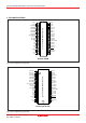
M37221M4H/M6H/M8H/MAH–XXXSP/FP M37221EASP/FP 1 42 P52/R VSYNC 2 41 P00/PWM0 P01/PWM1 P02/PWM2 3 40 4 39 P53/G P54/B P55/OUT1 5 38 P03/PWM3 P04/PWM4 6 37 P20/SCLK P21/SOUT 7 36 P22/SIN P05/PWM5 P06/INT2/A-D4 P07/INT1 8 35 10 P23/TIM3 11 P10/OUT2 P11/SCL1 P12/SCL2 P13/SDA1 P24/TIM2 12 P25 13 P26 14 P27 15 28 D-A 16 27 P16/A-D2 P17/A-D3 P30/A-D5/DA1 P32 17 26 P31/A-D6/DA2 CNVSS XIN XOUT VSS 18 25 19 24 20 23 RESET OSC1/P33 OSC2/P34 21 22 VCC 9 M37221EAS
M37221M4H/M6H/M8H/MAH–XXXSP/FP M37221EASP/FP Memory Map ■ M37221M4 H/M6H -XXXSP/FP 000016 1000016 Zero page M37221M6HXXXSP/FP RAM (448 bytes) M37221M4HXXXSP/FP RAM (384 bytes) 00C016 SFR area 11FFF16 00FF16 017F16 01BF16 02C016 02E016 02FF16 Not used Not used OSD RAM (96 bytes) (See note) OSD ROM (8K bytes) ROM correction function Vector 1: address 02C016 Vector 2: address 02E016 060016 06B716 Not used Not used A00016 M37221M6HXXXSP/FP ROM (24K bytes) C00016 M37221M4HXXXSP/FP ROM (16K byt
M37221M4H/M6H/M8H/MAH–XXXSP/FP M37221EASP/FP ■ M37221M8H/MAH-XXXSP/FP, M37221EASP/FP 1000016 000016 Zero page OSD ROM (8K bytes) 00C016 SFR area 00FF16 M37221MAHXXXSP/FP, M37221EASP/FP RAM (704 bytes) M37221M8HXXXSP/FP RAM (576 bytes) 11FFF16 01FF16 Not used 021716 021B16 2 page register Not used 02C016 02E016 02FF16 030016 033F16 03BF16 ROM correction function Vector 1: address 02C016 Vector 2: address 02E016 Not used OSD RAM (96 bytes) (See note) M37221MAHXXXSP/FP, M37221EASP/FP RAM (40K bytes
M37221M4H/M6H/M8H/MAH–XXXSP/FP M37221EASP/FP Memory Map of Special Function Register (SFR) ■ SFR area (addresses C016 to DF16) : State immediately after reset> 0 : “0” immediately after reset Function bit Name : 1 : “1” immediately after reset : No function bit 0 : Fix to this bit to “0” (do not write to “1”) ? : Indeterminate immediately after reset 1 : Fix to this bit to “1” (do not write to “0”) Address C016 C116 C216 C316 C416 C516 C616 C716 C816 C916 CA16 CB16 CC16 CD16 CE16
M37221M4H/M6H/M8H/MAH–XXXSP/FP M37221EASP/FP ■ SFR area (addresses E016 to FF16) : 0 : “0” immediately after reset Function bit Name : 1 : “1” immediately after reset : No function bit ? 0 : Fix to this bit to “0” (do not write to “1”) 1 : Fix to this bit to “1” (do not write to “0”) Address E016 E116 E216 E316 E416 E516 E616 E716 E816 E916 EA16 EB16 EC16 ED16 EE16 EF16 F016 F116 F216 F316 F416 F516 F616 F716 F816 F916 FA16 FB16 FC16 FD16 FE16 FF16
M37221M4H/M6H/M8H/MAH–XXXSP/FP M37221EASP/FP ■ 2 page register area (addresses 21716 to 21B16) : State immediately after reset> 0 : “0” immediately after reset Function bit Name : 1 : “1” immediately after reset : No function bit ? : Indeterminate immediately after reset 0 : Fix to this bit to “0” (do not write to “1”) 1 : Fix to this bit to “1” (do not write to “0”) Address 21716 21816 21916 21A16 21B16 Register Bit allocation b7 State immediately after reset b 0 b7 ROM correc
M37221M4H/M6H/M8H/MAH–XXXSP/FP M37221EASP/FP Internal State of Processor Status Register and Program Counter at Reset : Name 0 : “0” immediately after reset Function bit : 1 : “1” immediately after reset : No function bit ? : Indeterminate immediately after reset 0 : Fix to this bit to “0” (do not write to “1”) 1 : Fix to this bit to “1” (do not write to “0”) Register Bit allocation State immediately after reset b0 b7 b7 Processor status register
M37221M4H/M6H/M8H/MAH–XXXSP/FP M37221EASP/FP Structure of Register The figure of each register structure describes its functions, contents at reset, and attributes as follows: Bit position Bit attributes(Note 2) Values immediately after reset release (Note 1) CPU Mode Register b7 b6 b5 b4 b3 b2 b1 b0 0 0 1 1 CPU mode register (CPUM) (CM) [Address 00FB16] B Name 0, 1 Processor mode bits (CM0, CM1) Functions After reset R W 0 R W 1 RW 3, 4 Fix these bits to “1.
M37221M4H/M6H/M8H/MAH–XXXSP/FP M37221EASP/FP Addresses 00C116, 00C316, 00C516 Port Pi Direction Register b7 b6 b5 b4 b3 b2 b1 b0 Port Pi direction register (Di) (i=0,1,2) [Addresses 00C1 16, 00C316, 00C516] B Name Functions After reset R W 0 : Port Pi0 input mode 1 : Port Pi0 output mode 0 R W 1 0 : Port Pi1 input mode 1 : Port Pi1 output mode 0 R W 2 0 : Port Pi2 input mode 1 : Port Pi2 output mode 0 R W 3 0 : Port Pi3 input mode 1 : Port Pi3 output mode 0 R W 4 0 : Port Pi4 input mod
M37221M4H/M6H/M8H/MAH–XXXSP/FP M37221EASP/FP Address 00CB16 Port P5 Direction Register b7 b6 b5 b4 b3 b2 b1 b0 Port P5 direction register (D5) [Address 00CB16] b Name Functions After reset R W 0, 1 Nothing is assigned. These bits are write disable bits. When these bits are read out, the values are “0.
M37221M4H/M6H/M8H/MAH–XXXSP/FP M37221EASP/FP Address 00D516 PWM Output Control Register 1 b7 b6 b5 b4 b3 b2 b1 b0 PWM output control register 1 (PW) [Address 00D516] B Name Functions 0 DA, PWM count source 0 : Count source supply 1 : Count source stop selection bit (PW0) 0 : DA output 1 DA/PN4 selection bit 1 : PN4 output (PW1) After reset R W 0 R W 0 R W 2 P00/PWM0 output selection bit (PW2) 0: P00 output 1: PWM0 output 0 R W 3 P01/PWM1 output selection bit (PW3) 0: P01 output 1: PWM1 output 0 R
M37221M4H/M6H/M8H/MAH–XXXSP/FP M37221EASP/FP Address 00D716 I2C Data Shift Register b7 b6 b5 b4 b3 b2 b1 b0 I2C data shift register (S0) [Address 00D716 ] B 0 to 7 Name Functions D0 to D7 This is an 8-bit shift register to store receive data and write transmit data. After reset R W Indeterminate R W Note: To write data into the I2C data shift register after setting the MST bit to “0” (slave mode), keep an interval of 8 machine cycles or more.
M37221M4H/M6H/M8H/MAH–XXXSP/FP M37221EASP/FP Address 00D916 I2C Status Register b7 b6 b5 b4 b3 b2 b1 b0 I2C status register (S1) [Address 00D916] B 0 Name Functions Last receive bit (LRB) (See note) 0 : Last bit = “0 ” 1 : Last bit = “1 ” 1 General call detecting flag (AD0) (See note) 2 3 After reset R W Indeterminate R — 0 : No general call detected 1 : General call detected (See note) 0 R — Slave address comparison flag (AAS) (See note) 0 : Address mismatch 1 : Address match 0 R — Arbit
M37221M4H/M6H/M8H/MAH–XXXSP/FP M37221EASP/FP Address 00DB16 I2C Clock Control Register b7 b6 b5 b4 b3 b2 b1 b0 I2C clock control register (S2) [Address 00DB16] B 0 to 4 Name Functions After reset R W SCL frequency control bits Setup value of Standard clock High speed (CCR0 to CCR4) CCR4–CCR0 mode clock mode 0 0 to 0 2 0 R W Setup disabled Setup disabled 03 Setup disabled 04 Setup disabled 250 05 100 83.3 400 (See note) 06 333 166 ... 500/CCR value 1000/CCR value 1D 17.2 34.
M37221M4H/M6H/M8H/MAH–XXXSP/FP M37221EASP/FP Addresses 00DE16 and 00DF16 DA conversion register i b7 b6 b5 b4 b3 b2 b1 b0 0 DA conversion register i (i=1, 2) (DAi) [Addresses 00DE16, 00DF16] B Name After reset R W Functions 0 DA conversion to selection bit 5 (DAi0 to DAi5) b5 0 0 0 b4 0 0 0 b3 0 0 0 b2 0 0 0 b1 0 0 1 1 1 1 1 1 1 1 1 1 1 1 1 0 1 1 b0 0 : 0/64Vcc 1 : 1/64Vcc 0 : 2/64Vcc 0 R W 1 : 61/64Vcc 0 : 62/64Vcc 1 : 63/64Vcc 6 Fix this bit to “0.” 0 R W 7 Nothing is assigned.
M37221M4H/M6H/M8H/MAH–XXXSP/FP M37221EASP/FP Addresses 00E116 and 00E216 Vertical Position Register i b7 b6 b5 b4 b3 b2 b1 b0 Vertical position register i (CVi) (i = 1 and 2) [Addresses 00E1 16, 00E216] B Name Functions 0 to 6 Vertical display start positions 128 steps (0016 to 7F16) (CVi : CVi0 to CVi6) 7 Nothing is assigned. This bit is a write disable bit. When this bit is read out, the value is “0.
M37221M4H/M6H/M8H/MAH–XXXSP/FP M37221EASP/FP Address 00E516 Border Selection Register b7 b6 b5 b4 b3 b2 b1 b0 Border selection register (MD) [Address 00E5 16] B Name Functions After reset R W 0 Block 1 OUT1 output 0 : Same output as R, G, B is output Indeterminate R W border selection bit (MD10) 1 : Border output 1 Nothing is assigned. This bit is a write disable bit. When this bit is read out, the value is “0.
M37221M4H/M6H/M8H/MAH–XXXSP/FP M37221EASP/FP Address 00EA16 OSD Control Register b7 b6 b5 b4 b3 b2 b1 b0 OSD control register (CC) [Address 00EA 16] B Functions Name After reset R W 0 All-blocks display control bit (CC0) (See note) 0 : All-blocks display off 1 : All-blocks display on 0 R W 1 Block 1 display control bit (CC1) 0 : Block 1 display off 1 : Block 1 display on 0 R W 2 Block 2 display control bit (CC2) 0 : Block 2 display off 1 : Block 2 display on 0 R W 3 to 6 Nothing is as
M37221M4H/M6H/M8H/MAH–XXXSP/FP M37221EASP/FP Address 00ED16 OSD Clock Selection Register b7 b6 b5 b4 b3 b2 b1 b0 0 0 0 0 0 0 OSD clock selection register (CK) [Address 00ED16] B Name Functions After reset R W 0, 1 OSD clock Functions b1 b0 selection bits 0 0 The clock for display is supplied by connecting RC (CK0,CK1) or LC across the pins OSC1 and OSC2. 0 1 1 1 Since the main clock is used as the clock for display, the oscillation frequency is limited.
M37221M4H/M6H/M8H/MAH–XXXSP/FP M37221EASP/FP Address 00EF16 A-D Control Register 2 b7 b6 b5 b4 b3 b2 b1 b0 A-D control register 2 (AD2) [Address 00EF16] Name B D-A converter set bits (ADC0 to ADC5) 0 to 5 Functions b5 0 0 0 b4 0 0 0 b3 0 0 0 b2 0 0 0 b1 0 0 1 1 1 1 1 1 1 1 1 1 1 1 1 0 1 1 After re set R W b0 0 : 1/128Vcc 1 : 3/128Vcc 0 : 5/128Vcc 0 R W 0 R — 1 : 123/128Vcc 0 : 125/128Vcc 1 : 127/128Vcc 6, 7 Nothing is assigned. These bits are write disable bits.
M37221M4H/M6H/M8H/MAH–XXXSP/FP M37221EASP/FP Address 00F516 Timer 34 Mode Register b7 b6 b5 b4 b3 b2 b1 b0 Timer 34 mode register (T34M) [Address 00F516] B Name 0 Timer 3 count source selection bit (T34M0) 1 Timer 4 internal interrupt count source selection bit (T34M1) Functions After reset R W 0 R W 0 : f(XIN)/16 1 : External clock source 0 : Timer 3 overflow signal 1 : f(XIN)/16 0 R W 2 Timer 3 count stop bit (T34M2) 0: Count start 1: Count stop 0 R W 3 Timer 4 count stop bit (T34M3) 0: Count
M37221M4H/M6H/M8H/MAH–XXXSP/FP M37221EASP/FP Address 00FB16 CPU Mode Register b7 b6 b5 b4 b3 b2 b1 b0 1 1 1 1 1 0 0 CPU mode register (CM) [Address 00FB16] B Name Functions 0, 1 Fix these bits to “0.” Stack page selection bit (CM2) (See note) 2 After reset R W Indeterminate R W 1 RW Indeterminate R W 0: 0 page 1: 1 page 3 to 7 Fix these bits to “1.” Note: This bit is set to “1” after the reset release.
M37221M4H/M6H/M8H/MAH–XXXSP/FP M37221EASP/FP Address 00FD16 Interrupt Request Register 2 b7 b6 b5 b4 b3 b2 b1 b0 0 Interrupt request register 2 (IREQ2) [Address 00FD16] B Name 0 INT1 external interrupt request bit (IT1R) 1 INT2 external interrupt request bit (IT2R) 2 Serial I/O interrupt request bit (S1R) Functions After reset R W 0 : No interrupt request issued 0 R ✽ 1 : Interrupt request issued 0 : No interrupt request issued 0 R ✽ 1 : Interrupt request issued 0 : No interrupt request issued 1 : I
M37221M4H/M6H/M8H/MAH–XXXSP/FP M37221EASP/FP Address 00FF16 Interrupt Control Register 2 b7 b6 b5 b4 b3 b2 b1 b0 0 0 0 0 Interrupt control register 2 (ICON2) [Address 00FF16] B Name 0 INT1 external interrupt enable bit (IT1E) 1 INT2 external interrupt enable bit (IT2E) 2 Serial I/O interrupt enable bit (S1E) 3 Fix this bit to “0.
M37221M4H/M6H/M8H/MAH–XXXSP/FP M37221EASP/FP 20. PACKAGE OUTLINE MMP 42P4B EIAJ Package Code SDIP42-P-600-1.78 Plastic 42pin 600mil SDIP Weight(g) 4.1 Lead Material Alloy 42/Cu Alloy 22 1 21 E 42 e1 c JEDEC Code – Symbol A A1 A2 b b1 b2 c D E e e1 L L A1 A A2 D e b1 b2 b SEATING PLANE 42P2R-A/E Dimension in Millimeters Min Nom Max – – 5.5 0.51 – – – 3.8 – 0.35 0.45 0.55 0.9 1.0 1.3 0.63 0.73 1.03 0.22 0.27 0.34 36.5 36.7 36.9 12.85 13.0 13.15 – 1.778 – – 15.24 – 3.
REVISION HISTORY Rev. M37221M4H/M6H/M8H/MAH–XXXSP/FP M37221EASP/FP Date Description Summary Page 1.
Sales Strategic Planning Div. Nippon Bldg., 2-6-2, Ohte-machi, Chiyoda-ku, Tokyo 100-0004, Japan Keep safety first in your circuit designs! 1. Renesas Technology Corp. puts the maximum effort into making semiconductor products better and more reliable, but there is always the possibility that trouble may occur with them. Trouble with semiconductors may lead to personal injury, fire or property damage.