
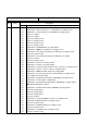
Specifications
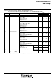

83
SINGLE-CHIP 8-BIT CMOS MICROCOMPUTER
MITSUBISHI MICROCOMPUTERS
7560 Group
SWITCHING CHARACTERISTICS (Extended operating temperature version)
Table 54 Switching characteristics 1 (Extended operating temperature version)
(VCC = 4.0 to 5.5 V, VSS = 0 V, Ta = –40 to 85°C, unless otherwise noted)
Notes1: When the P45/TXD P-channel output disable bit of the UART control register (bit 4 of address 001B16) is “0”.
2: X
OUT and XCOUT pins are excluded.
Serial I/O1 clock output “H” pulse width
Serial I/O1 clock output “L” pulse width
Serial I/O1 output delay time (Note 1)
Serial I/O1 output valid time (Note 1)
Serial I/O1 clock output rising time
Serial I/O1 clock output falling time
Serial I/O2 clock output “H” pulse width
Serial I/O2 clock output “L” pulse width
Serial I/O2 output delay time
Serial I/O2 output valid time
Serial I/O2 clock output falling time
CMOS output rising time (Note 2)
CMOS output falling time (Note 2)
140
30
30
0.2 ✕ tC (SCLK2)
40
30
30
Symbol Parameter
Limits
Min.
ns
ns
ns
ns
ns
ns
ns
ns
ns
ns
ns
ns
ns
Unit
tC (SCLK1)/2–30
tC (SCLK1)/2–30
–30
10
10
Typ.
Max.
t
wH(SCLK1)
twL(SCLK1)
td(SCLK1–TXD)
tv(SCLK1–TXD)
tr(SCLK1)
tf(SCLK1)
twH(SCLK2)
twL(SCLK2)
t
d(S
CLK2
–S
OUT2
)
t
v(S
CLK2
–S
OUT2
)
tf(SCLK2)
tr(CMOS)
tf(CMOS)
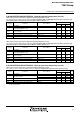
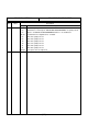
Table 55 Switching characteristics 2 (Extended operating temperature version)
(VCC = 2.5 to 4.0 V, VSS = 0 V, Ta = –20 to 85°C, and VCC = 3.0 to 5.5 V, Ta = –40 to –20°C, unless otherwise noted)
ns
ns
ns
ns
ns
ns
ns
ns
ns
ns
ns
ns
ns
Unit
Notes1: When the P45/TXD P-channel output disable bit of the UART control register (bit 4 of address 001B16) is “0”.
2: X
OUT and XCOUT pins are excluded.
Serial I/O1 clock output “H” pulse width
Serial I/O1 clock output “L” pulse width
Serial I/O1 output delay time (Note 1)
Serial I/O1 output valid time (Note 1)
Serial I/O1 clock output rising time
Serial I/O1 clock output falling time
Serial I/O2 clock output “H” pulse width
Serial I/O2 clock output “L” pulse width
Serial I/O2 output delay time
Serial I/O2 output valid time
Serial I/O2 clock output falling time
CMOS output rising time (Note 2)
CMOS output falling time (Note 2)
350
50
50
0.2 ✕ tC (SCLK2)
50
50
50
Symbol Parameter
Limits
Min.
tC (SCLK1)/2–50
tC (SCLK1)/2–50
–30
20
20
Max.
twH(SCLK1)
twL(SCLK1)
td(SCLK1–TXD)
tv(SCLK1–TXD)
tr(SCLK1)
tf(SCLK1)
twH(SCLK2)
twL(SCLK2)
t
d(S
CLK2
–S
OUT2
)
t
v(S
CLK2
–S
OUT2
)
tf(SCLK2)
tr(CMOS)
tf(CMOS)
Typ.
tC (SCLK2)/2–160
tC (SCLK2)/2–160
0
t
C
(S
CLK2
)/2–240
t
C
(S
CLK2
)/2–240
0
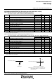
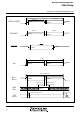
Fig. 69 Circuit for measuring output switching characteristics
M
easurement output p
i
n
1
0
0
p
F
C
M
O
S
o
u
t
p
u
t
N
o
t
e
:
W
h
e
n
P
7
1
–
P
7
7
,
P
4
0
a
n
d
b
i
t
4
o
f
t
h
e
U
A
R
T
c
o
n
t
r
o
l
r
e
g
i
s
t
e
r
(
a
d
d
r
e
s
s
0
0
1
B
1
6
)
i
s
“
1
”
(
N
-
c
h
a
n
n
e
l
o
p
e
n
-
d
r
a
i
n
o
u
t
p
u
t
m
o
d
e
)
.
N
-
c
h
a
n
n
e
l
o
p
e
n
-
d
r
a
i
n
o
u
t
p
u
t
(
N
o
t
e
)
1
k
Ω
1
0
0
p
F
M
easurement output p
i
n