
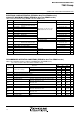
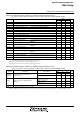
Specifications

76
SINGLE-CHIP 8-BIT CMOS MICROCOMPUTER
7560 Group
MITSUBISHI MICROCOMPUTERS
SWITCHING CHARACTERISTICS (EPROM or One Time PROM version)
Table 41 Switching characteristics 1 (EPROM or One Time PROM version)
(VCC = 4.0 to 5.5 V, VSS = 0 V, Ta = –20 to 85°C, unless otherwise noted)
Notes1: When the P45/TXD P-channel output disable bit of the UART control register (bit 4 of address 001B16) is “0”.
2: X
OUT and XCOUT pins are excluded.
Serial I/O1 clock output “H” pulse width
Serial I/O1 clock output “L” pulse width
Serial I/O1 output delay time (Note 1)
Serial I/O1 output valid time (Note 1)
Serial I/O1 clock output rising time
Serial I/O1 clock output falling time
Serial I/O2 clock output “H” pulse width
Serial I/O2 clock output “L” pulse width
Serial I/O2 output delay time
Serial I/O2 output valid time
Serial I/O2 clock output falling time
CMOS output rising time (Note 2)
CMOS output falling time (Note 2)
140
30
30
0.2 ✕ tC (SCLK2)
40
30
30
Symbol Parameter
Limits
Min.
ns
ns
ns
ns
ns
ns
ns
ns
ns
ns
ns
ns
ns
Unit
tC (SCLK1)/2–30
tC (SCLK1)/2–30
–30
10
10
Typ.
Max.
twH(SCLK1)
twL(SCLK1)
td(SCLK1–TXD)
tv(SCLK1–TXD)
tr(SCLK1)
tf(SCLK1)
twH(SCLK2)
twL(SCLK2)
t
d(S
CLK2
–S
OUT2
)
t
v(S
CLK2
–S
OUT2
)
tf(SCLK2)
tr(CMOS)
tf(CMOS)
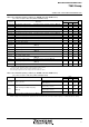
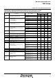
Table 42 Switching characteristics 2 (EPROM or One Time PROM version)
(VCC = 2.5 to 4.0 V, VSS = 0 V, Ta = –20 to 85°C, unless otherwise noted)
ns
ns
ns
ns
ns
ns
ns
ns
ns
ns
ns
ns
ns
Unit
Notes1: When the P45/TXD P-channel output disable bit of the UART control register (bit 4 of address 001B16) is “0”.
2: X
OUT and XCOUT pins are excluded.
Serial I/O1 clock output “H” pulse width
Serial I/O1 clock output “L” pulse width
Serial I/O1 output delay time (Note 1)
Serial I/O1 output valid time (Note 1)
Serial I/O1 clock output rising time
Serial I/O1 clock output falling time
Serial I/O2 clock output “H” pulse width
Serial I/O2 clock output “L” pulse width
Serial I/O2 output delay time
Serial I/O2 output valid time
Serial I/O2 clock output falling time
CMOS output rising time (Note 2)
CMOS output falling time (Note 2)
350
50
50
0.2 ✕ tC (SCLK2)
50
50
50
Symbol Parameter
Limits
Min.
tC (SCLK1)/2–50
tC (SCLK1)/2–50
–30
20
20
Max.
twH(SCLK1)
twL(SCLK1)
td(SCLK1–TXD)
tv(SCLK1–TXD)
tr(SCLK1)
tf(SCLK1)
twH(SCLK2)
twL(SCLK2)
t
d(S
CLK2
–S
OUT2
)
t
v(S
CLK2
–S
OUT2
)
tf(SCLK2)
tr(CMOS)
tf(CMOS)
Typ.
tC (SCLK2)/2–160
tC (SCLK2)/2–160
0
t
C
(S
CLK2
)/2–240
t
C
(S
CLK2
)/2–240
0