
Specifications

SINGLE-CHIP 8-BIT CMOS MICROCOMPUTER
MITSUBISHI MICROCOMPUTERS
7560 Group
4
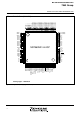
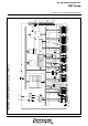
PIN DESCRIPTION
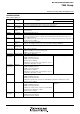
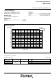
Table 1 Pin description (1)
V
CC, VSS
FunctionPin Name
Function except a port function
•LCD segment output pins
Power source •Apply voltage of 2.2 V to 5.5 V (2.5 to 5.5 V for EPROM and One Time PROM version, 3.0 to 5.5 V
for extended operating temperature version) to VCC, and 0 V to VSS.
VREF
AVSS
RESET
XIN
XOUT
VL1–VL3
C1, C2
COM
0
–COM
3
SEG
0
–SEG
17
P00/SEG26–
P07/SEG33
P10/SEG34–
P15/SEG39
P16, P17
P20 – P27
P3
0
/SEG
18
–
P3
7
/SEG
25
Analog refer-
ence voltage
Analog power
source
Reset input
Clock input
Clock output
LCD power
source
Charge-pump
capacitor pin
Common output
Segment output
I/O port P0
I/O port P1
I/O port P2
Output port P3
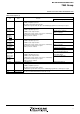
•Reference voltage input pin for A-D converter and D-A converter.
•GND input pin for A-D converter and D-A converter.
•Connect to VSS.
•Reset input pin for active “L”.
•Input and output pins for the main clock generating circuit.
•Connect a ceramic resonator or a quartz-crystal oscillator between the XIN and XOUT pins to set
the oscillation frequency.
•If an external clock is used, connect the clock source to the XIN pin and leave the XOUT pin open. A
feedback resistor is built-in.
•Input 0 ≤ VL1 ≤ VL2 ≤ VL3 voltage.
•Input 0 – VL3 voltage to LCD. (0 ≤ VL1 ≤ VL2 ≤ VL3 when a voltage is multiplied.)
•External capacitor pins for a voltage multiplier (3 times) of LCD control.
•LCD common output pins.
•COM2 and COM3 are not used at 1/2 duty ratio.
•COM3 is not used at 1/3 duty ratio.
•LCD segment output pins.
•8-bit I/O port.
•CMOS compatible input level.
•CMOS 3-state output structure.
•Pull-up control is enabled.
•I/O direction register allows each 8-bit pin to be pro-
grammed as either input or output.
•6-bit I/O port.
•CMOS compatible input level.
•CMOS 3-state output structure.
•Pull-up control is enabled.
•I/O direction register allows each 6-bit pin to be pro-
grammed as either input or output.
•2-bit I/O port.
•CMOS compatible input level.
•CMOS 3-state output structure.
•I/O direction register allows each pin to be individually programmed as either input or output.
•Pull-up control is enabled.
•8-bit I/O port.
•CMOS compatible input level.
•CMOS 3-state output structure.
•I/O direction register allows each pin to be individually
programmed as either input or output.
•Pull-up control is enabled.
•8-bit output.
•CMOS 3-state output structure.
•Port output control is enabled.
•Key input (key-on wake-up) interrupt
input pins
•LCD segment output pins