
Specifications

SINGLE-CHIP 8-BIT CMOS MICROCOMPUTER
MITSUBISHI MICROCOMPUTERS
7560 Group
47
(frequency of count source for LCDCK)
(divider division ratio for LCD)
f(LCDCK)=
f(LCDCK)
duty ratio
Frame frequency=
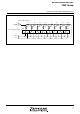
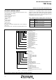
Fig. 49 LCD display RAM map
Common Pin and Duty Ratio Control
The common pins (COM0–COM3) to be used are determined by
duty ratio.
Select duty ratio by the duty ratio selection bits (bits 0 and 1 of the
LCD mode register).
After reset, the VCC (VL3) voltage is output from the common pins.
LCD Display RAM
Addresses 004016 to 005316 are the designated RAM for the LCD
display. When “1” are written to these addresses, the correspond-
ing segments of the LCD display panel are turned on.
LCD Drive Timing
The frequency of internal signal LCDCK decided LCD drive timing
and the frame frequency can be determined with the following
equation:
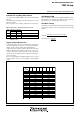
Table 13 Duty ratio control and common pins used
Duty
ratio
2
3
4
Common pins used
Notes 1: COM2 and COM3 are open.
2: COM3 is open.
Bit 1
0
1
1
Bit 0
1
0
1
COM0, COM1 (Note 1)
COM0–COM2 (Note 2)
COM0–COM3
Duty ratio selection bits
Segment Signal Output Pins
Segment signal output pins are classified into the segment-only
pins (SEG0–SEG17), the segment or output port pins (SEG18–
SEG25), and the segment or I/O port pins (SEG26–SEG39).
Segment signals are output according to the bit data of the LCD
RAM corresponding to the duty ratio. After reset, a VCC (=VL3)
voltage is output to the segment-only pins and the segment/out-
put port pins are the high impedance condition and pulled up to
VCC (=VL3) voltage.
Also, the segment/I/O port pins(SEG26–SEG39) are set to input
mode as I/O ports, and VCC (=VL3) is applied to them by pull-up
resistor.
0
0
4
01
6
0
0
4
11
6
0
0
4
21
6
0
0
4
31
6
0
0
4
41
6
0
0
4
51
6
0
0
4
61
6
0
0
4
71
6
0
0
4
81
6
0
0
4
91
6
0
0
4
A1
6
0
0
4
B1
6
0
0
4
C1
6
0
0
4
D1
6
0
0
4
E1
6
0
0
4
F1
6
0
0
5
01
6
0
0
5
11
6
0
0
5
21
6
0
0
5
31
6
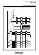
B
i
t
A
d
d
r
e
s
s
S
E
G
1
S
E
G3
S
E
G5
S
E
G7
S
E
G9
S
E
G1
1
S
E
G1
3
S
E
G1
5
S
E
G1
7
S
E
G1
9
S
E
G2
1
S
E
G2
3
S
E
G2
5
S
E
G2
7
S
E
G2
9
S
E
G3
1
S
E
G3
3
S
E
G3
5
S
E
G3
7
S
E
G3
9
76543210
C
O
M
3
C
O
M
0
C
O
M
2
C
O
M
1
C
O
M
0
COM
3
COM
2
C
O
M
1
SEG
0
SEG2
SEG4
SEG6
SEG8
SEG10
SEG12
SEG14
SEG16
SEG18
SEG20
SEG22
SEG24
SEG26
SEG28
SEG30
SEG32
SEG34
SEG36
SEG38