
Specifications

SINGLE-CHIP 8-BIT CMOS MICROCOMPUTER
MITSUBISHI MICROCOMPUTERS
7560 Group
46
Voltage Multiplier (3 Times)
The voltage multiplier performs threefold boosting. This circuit in-
puts a reference voltage for boosting from LCD power input pin
V
L1.
Set each bit of the segment output enable register and the LCD
mode register in the following order for operating the voltage mul-
tiplier.
1. Set the segment output enable bits (bits 0 to 5) of the seg-
ment output enable register to “0” or “1”.
2. Set the duty ratio selection bits (bits 0 and 1), the bias con-
trol bit (bit 2), the LCD circuit divider division ratio selection
bits (bits 5 and 6), and the LCDCK count source selection
bit (bit 7) of the LCD mode register to “0” or “1”.
3. Set the LCD output enable bit (bit 6) of the segment output
enable register to “1”. Apply the limit voltage or less to the
V
L1 pin.
4. Set the voltage multiplier control bit (bit 4) of the LCD mode
register to “1”. However, be sure to select 1/3 bias for bias
control.
When voltage is input to the VL1 pin during operating the voltage
multiplier, voltage that is twice as large as VL1 occurs at the VL2
pin, and voltage that is three times as large as VL1 occurs at the
VL3 pin.
■Notes on Voltage Multiplier
When using the voltage multiplier, apply the limit voltage or less to
the VL1 pin, then set the voltage multiplier control bit to “1” (en-
abled).
When not using the voltage multiplier, set the LCD output enable
bit to “1”, then apply proper voltage to the LCD power input pins
(VL1–VL3).
When the LCD output enable bit is set to “0” (disabled), the VCC
voltage is applied to the VL3 pin inside of this microcomputer.
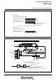
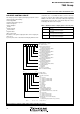
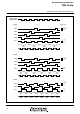
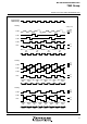
Fig. 48 Example of circuit at each bias
Table 12 Bias control and applied voltage to VL1–VL3
Bias value
1/3 bias
1/2 bias
Voltage value
VL3=VLCD
VL2=2/3 VLCD
VL1=1/3 VLCD
VL3=VLCD
VL2=VL1=1/2 VLCD
Note : VLCD is the maximum value of supplied voltage for the
LCD panel.
Bias Control and Applied Voltage to LCD
Power Input Pins
To the LCD power input pins (VL1–VL3), apply the voltage shown
in Table 12 according to the bias value.
Select a bias value by the bias control bit (bit 2 of the LCD mode
register).
V
L3
V
L
2
C
2
C
1
V
L
1
1
/
3
b
i
a
s
w
h
e
n
u
s
i
n
g
t
h
e
v
o
l
t
a
g
e
m
u
l
t
i
p
l
i
e
r
V
L3
V
L2
C
2
C
1
V
L1
1
/
3
b
i
a
s
w
h
e
n
n
o
t
u
s
i
n
g
t
h
e
v
o
l
t
a
g
e
m
u
l
t
i
p
l
i
e
r
O
p
e
n
O
p
e
n
R
2
R
1
R
3
R
1=
R
2=
R
3
C
o
n
t
r
a
s
t
c
o
n
t
r
o
l
V
L
3
V
L
2
C
2
C
1
V
L
1
1/2
bi
as
O
p
e
n
O
p
e
n
R
4
R
5
R
4
=
R
5
C
o
n
t
r
a
s
t
c
o
n
t
r
o
l
P
X
x