
Specifications

SINGLE-CHIP 8-BIT CMOS MICROCOMPUTER
MITSUBISHI MICROCOMPUTERS
7560 Group
44
LCD DRIVE CONTROL CIRCUIT
The 7560 group has the Liquid Crystal Display (LCD) drive control
circuit consisting of the following.
•
LCD display RAM
•
Segment output enable register
•
LCD mode register
•
Voltage multiplier
•
Selector
•
Timing controller
•
Common driver
•
Segment driver
•
Bias control circuit
A maximum of 40 segment output pins and 4 common output pins
can be used.
Up to 160 pixels can be controlled for LCD display. When the LCD
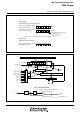
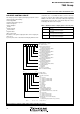
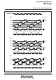
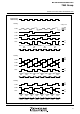
Fig. 46 Structure of segment output enable register and LCD mode register
enable bit is set to “1” (LCD ON) after data is set in the LCD mode
register, the segment output enable register and the LCD display
RAM, the LCD drive control circuit starts reading the display data
automatically, performs the bias control and the duty ratio control,
and displays the data on the LCD panel.
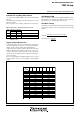
Table 11 Maximum number of display pixels at each duty ratio
Duty ratio Maximum number of display pixel
80 dots
or 8 segment LCD 10 digits
120 dots
or 8 segment LCD 15 digits
160 dots
or 8 segment LCD 20 digits
2
3
4
S
egment output ena
bl
e
bi
t 0
0 : Output ports P3
0–P35
1 : Segment output SEG18–SEG23
Segment output enable bit 1
0 : Output ports P3
6, P37
1 : Segment output SEG24,SEG25
Segment output enable bit 2
0 : I/O ports P0
0–P05
1 : Segment output SEG26–SEG31
Segment output enable bit 3
0 : I/O ports P0
6,P07
1 : Segment output SEG32,SEG33
Segment output enable bit 4
0 : I/O port P1
0
1 : Segment output SEG34
Segment output enable bit 5
0 : I/O ports P1
1–P15
1 : Segment output SEG35–SEG39
LCD output enable bit
0 : Disabled
1 : Enabled
Not used (“0” at reading)
(Write “0” to this bit at writing.)
S
egment output ena
bl
e reg
i
ster
(SEG : address 0038
16)
b
7
b
0
LCD
mo
d
e reg
i
ster
(LM : address 0039
16)
D
uty rat
i
o se
l
ect
i
on
bi
ts
b1b0
0 0 : Not used
0 1 : 2 duty (use COM
0, COM1)
1 0 : 3 duty (use COM
0–COM2)
1 1 : 4 duty (use COM
0–COM3)
Bias control bit
0 : 1/3 bias
1 : 1/2 bias
LCD enable bit
0 : LCD OFF
1 : LCD ON
Voltage multiplier control bit
0 : Voltage multiplier disable
1 : Voltage multiplier enable
LCD circuit divider division ratio selection bits
b6b5
0 0 : Clock input
0 1 : 2 division of Clock input
1 0 : 4 division of Clock input
1 1 : 8 division of Clock input
LCDCK count source selection bit (Note)
0 : f(X
CIN)/32
1 : f(X
IN)/8192 (f(XCIN)/8192 in low-speed mode)
N
ote :
LCDCK
i
s a c
l
oc
k
f
or a
LCD
t
i
m
i
ng contro
ll
er.
b
7
b
0
0