
Specifications
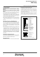

SINGLE-CHIP 8-BIT CMOS MICROCOMPUTER
MITSUBISHI MICROCOMPUTERS
7560 Group
40
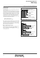
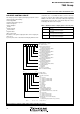
A-D CONVERTER
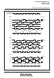
[A-D Conversion Low-Order Register (ADL)]
0014
16
[A-D Conversion High-Order Register (ADH)]
0035
16
The A-D conversion registers are read-only registers that store the
result of an A-D conversion . When reading this register during an
A-D conversion, the previous conversion result is read.
The high-order 8 bits of a conversion result is stored in the A-D
conversion high-order register (address 003516), and the low-or-
der 2 bits of the same result are stored in bit 7 and bit 6 of the A-D
conversion low-order register (address 001416).
Bit 0 of the A-D conversion low-order register is the conversion
mode selection bit. When this bit is set to “0”, that becomes the
10-bit A-D mode. When this bit is set to “1”, that becomes the 8-bit
A-D mode.
[A-D Control Register (ADCON)] 003416
The A-D control register controls the A-D conversion process. Bits
0 to 2 of this register select specific analog input pins. Bit 3 indi-
cates the completion of an A-D conversion. The value of this bit re-
mains at “0” during an A-D conversion, then it is set to “1” when
the A-D conversion is completed. Writing “0” to this bit starts the
A-D conversion.
Bit 4 is the VREF input switch bit which controls connection of the
resistor ladder and the reference voltage input pin (VREF). The
resistor ladder is always connected to VREF when bit 4 is set to
“1”. When bit 4 is set to “0”, the resistor ladder is cut off from VREF
except for A-D conversion performed. When bit 5, which is the AD
external trigger valid bit, is set to “1”, A-D conversion starts also by
a falling edge of an ADT input. When using an A-D external trigger,
set the P57/ADT pin to input mode (set “0” to bit 7 of port P5 direc-
tion register).
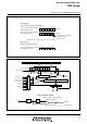
Comparison Voltage Generator
The comparison voltage generator divides the voltage between
AVSS and VREF by 256 (when 8-bit A-D mode) or 1024 (when 10-
bit A-D mode), and outputs the divided voltages.
Channel Selector
The channel selector selects one of the input ports P6
7
/AN
7
–P6
0
/AN
0
.
Comparator and Control Circuit
The comparator and control circuit compare an analog input volt-
age with the comparison voltage and store the result in the A-D
conversion register. When an A-D conversion is completed, the
control circuit sets the AD conversion completion bit and the AD
converter interrupt request bit to “1”.
Note that because the comparator consists of a capacitor
coupling, set f(XIN) to 500 kHz or more during an A-D conversion.
Use the clock divided from the main clock f(X
IN) as the system clock
φ.
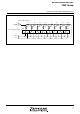
Fig. 40 Structure of A-D converter-related registers
A
-
D
c
o
n
t
r
o
l
r
e
g
i
s
t
e
r
(
A
D
C
O
N
:
a
d
d
r
e
s
s
0
0
3
4
1
6)
AD
convers
i
on comp
l
et
i
on
bi
t
0 : Conversion in progress
1 : Conversion completed
A
na
l
og
i
nput p
i
n se
l
ect
i
on
bi
ts
b2b1b0
0 0 0 : P60/AN0
0 0 1 : P61/AN1
0 1 0 : P62/AN2
0 1 1 : P63/AN3
1 0 0 : P64/AN4
1 0 1 : P65/AN5
1 1 0 : P66/AN6
1 1 1 : P67/AN7
V
R
E
F
i
n
p
u
t
s
w
i
t
c
h
b
i
t
0
:
A
U
T
O
1
:
O
N
AD
externa
l
tr
i
gger va
lid
bi
t
0 : A-D external trigger invalid
1 : A-D external trigger valid
b
7
b
0
I
nterrupt source se
l
ect
i
on
bi
t
0 : Interrupt request at A-D
conversion completed
1 : Interrupt request at ADT
input falling
N
ot use
d
(
“0” at rea
di
ng
)
A
-
D
c
o
n
v
e
r
s
i
o
n
l
o
w
-
o
r
d
e
r
r
e
g
i
s
t
e
r
(
A
D
L
:
a
d
d
r
e
s
s
0
0
1
4
1
6)
C
onvers
i
on mo
d
e se
l
ect
i
on
bi
t
0 : 10-bit A-D mode
1 : 8-bit A-D mode
Not used (“0” at reading)
•For
10-bit A-D mode
A-D conversion result
•For 8-bit A-D mode
Not used (undefined at reading)
b
7
b
0