
Specifications

SINGLE-CHIP 8-BIT CMOS MICROCOMPUTER
MITSUBISHI MICROCOMPUTERS
7560 Group
33
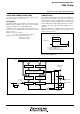
(2) Asynchronous Serial I/O (UART) Mode
Clock asynchronous serial I/O mode (UART) is selected by setting
the serial I/O1 mode selection bit of the serial I/O1 control register
to “0”.
Eight serial data transfer formats can be selected, and the transfer
formats used by a transmitter and receiver must be identical.
The transmit and receive shift registers each have a buffer regis-
ter, but the two buffers have the same address (001816) in
memory. Since the shift register cannot be written to or read from
directly, transmit data is written to the transmit buffer, and receive
data is read from the receive buffer.
The transmit buffer can also hold the next data to be transmitted
during transmitting, and the receive buffer register can hold re-
ceived one-byte data while the next one-byte data is being re-
ceived.
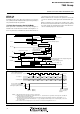
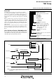
Fig. 30 Block diagram of UART serial I/O1
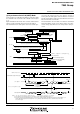
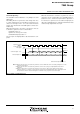
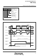
Fig. 31 Operation of UART serial I/O1 function
X
IN
1/4
O
E
P
E
F
E
1/16
1
/
1
6
D
ata
b
us
R
e
c
e
i
v
e
b
u
f
f
e
r
r
e
g
i
s
t
e
r
A
d
d
r
e
s
s
0
0
1
8
1
6
R
ece
i
ve s
hif
t reg
i
ster
R
e
c
e
i
v
e
b
u
f
f
e
r
f
u
l
l
f
l
a
g
(
R
B
F
)
R
e
c
e
i
v
e
i
n
t
e
r
r
u
p
t
r
e
q
u
e
s
t
B
a
u
d
r
a
t
e
g
e
n
e
r
a
t
o
r
F
r
e
q
u
e
n
c
y
d
i
v
i
s
i
o
n
r
a
t
i
o
1
/
(
n
+
1
)
Add
ress 001
C
16
S
T
/
S
P
/
P
A
g
e
n
e
r
a
t
o
r
Transmit buffer register
D
a
t
a
b
u
s
T
r
a
n
s
m
i
t
s
h
i
f
t
r
e
g
i
s
t
e
r
Add
ress 001816
T
r
a
n
s
m
i
t
s
h
i
f
t
r
e
g
i
s
t
e
r
s
h
i
f
t
c
o
m
p
l
e
t
i
o
n
f
l
a
g
(
T
S
C
)
T
r
a
n
s
m
i
t
b
u
f
f
e
r
e
m
p
t
y
f
l
a
g
(
T
B
E
)
T
ransm
i
t
i
nterrupt request
Add
ress 001916
S
T
d
e
t
e
c
t
o
r
SP
d
etector
U
A
R
T
c
o
n
t
r
o
l
r
e
g
i
s
t
e
r
Add
ress 001
B
16
Ch
aracter
l
engt
h
se
l
ect
i
on
bi
t
A
d
d
r
e
s
s
0
0
1
A
1
6
B
R
G
c
o
u
n
t
s
o
u
r
c
e
s
e
l
e
c
t
i
o
n
b
i
t
T
ransm
i
t
i
nterrupt source se
l
ect
i
on
bit
S
e
r
i
a
l
I
/
O
1
s
y
n
c
h
r
o
n
i
z
a
t
i
o
n
c
l
o
c
k
s
e
l
e
c
t
i
o
n
b
i
t
Cl
oc
k
contro
l
c
i
rcu
it
C
h
a
r
a
c
t
e
r
l
e
n
g
t
h
s
e
l
e
c
t
i
o
n
b
i
t
7
b
i
t
s
8
b
i
t
s
S
e
r
i
a
l
I
/
O
1
c
o
n
t
r
o
l
r
e
g
i
s
t
e
r
P
46/
S
CLK1
S
e
r
i
a
l
I
/
O
1
s
t
a
t
u
s
r
e
g
i
s
t
e
r
P
44/
R
X
D
P
45/
T
X
D
T
S
C
=
“
0
”
T
B
E
=
“
1
”
R
B
F
=
“
0
”
T
B
E
=
“
0
”
TBE
= “0”
R
B
F
=
“
1
”
RBF
= “1”
S
T
D
0
D
1
S
P
D
0
D
1
ST
S
P
T
B
E
=
“
1
” TSC = “1”
✽
ST
D
0
D
1
SP
D
0
D
1
S
T
S
P
T
ransm
i
t
b
u
ff
er reg
i
ster wr
i
te s
i
gna
l
✽
Generated at 2nd bit in 2-stop-bit mode
1 start
bi
t
7 or 8 data bits
1 or 0 parity bit
1 or 2 stop bit (s)
1
:
E
r
r
o
r
f
l
a
g
d
e
t
e
c
t
i
o
n
o
c
c
u
r
s
a
t
t
h
e
s
a
m
e
t
i
m
e
t
h
a
t
t
h
e
R
B
F
f
l
a
g
b
e
c
o
m
e
s
“
1
”
(
a
t
1
s
t
s
t
o
p
b
i
t
f
o
r
r
e
c
e
p
t
i
o
n
)
.
2
:
T
h
e
s
e
r
i
a
l
I
/
O
1
r
e
c
e
i
v
e
i
n
t
e
r
r
u
p
t
r
e
q
u
e
s
t
o
c
c
u
r
s
w
h
e
n
t
h
e
r
e
c
e
i
v
e
b
u
f
f
e
r
f
u
l
l
f
l
a
g
(
R
B
F
)
b
e
c
o
m
e
s
“
1
”
.
3
:
S
e
l
e
c
t
t
h
e
s
e
r
i
a
l
I
/
O
1
t
r
a
n
s
m
i
t
i
n
t
e
r
r
u
p
t
r
e
q
u
e
s
t
o
c
c
u
r
r
e
n
c
e
f
a
c
t
o
r
b
e
t
w
e
e
n
w
h
e
n
t
h
e
t
r
a
n
s
m
i
t
b
u
f
f
e
r
r
e
g
i
s
t
e
r
h
a
s
e
m
p
t
i
e
d
(
T
B
E
=
“
1
”
)
o
r
a
f
t
e
r
t
h
e
t
r
a
n
s
m
i
t
s
h
i
f
t
o
p
e
r
a
t
i
o
n
h
a
s
e
n
d
e
d
(
T
S
C
=
“
1
”
)
,
b
y
s
e
t
t
i
n
g
t
h
e
t
r
a
n
s
m
i
t
i
n
t
e
r
r
u
p
t
s
o
u
r
c
e
s
e
l
e
c
t
i
o
n
b
i
t
(
T
I
C
)
o
f
t
h
e
s
e
r
i
a
l
I
/
O
1
c
o
n
t
r
o
l
r
e
g
i
s
t
e
r
.
N
o
t
e
s
S
e
r
i
a
l
o
u
t
p
u
t
T
x
D
S
e
r
i
a
l
i
n
p
u
t
R
x
D
R
ece
i
ve
b
u
ff
er reg
i
ster rea
d
s
i
gna
l
T
ransm
i
t or rece
i
ve c
l
oc
k
(N
otes 1,
2)
(N
otes 1,
2)