
Specifications

SINGLE-CHIP 8-BIT CMOS MICROCOMPUTER
MITSUBISHI MICROCOMPUTERS
7560 Group
26
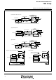
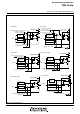
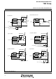
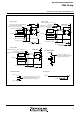
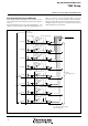
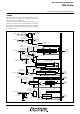
Key Input Interrupt (Key-on Wake Up)
The key input interrupt is enabled when any of port P2 is set to in-
put mode and the bit corresponding to key input control register is
set to “1”.
A Key input interrupt request is generated by applying “L” level
voltage to any pin of port P2 of which key input interrupt is en-
abled. In other words, it is generated when AND of input level
goes from “1” to “0”. A connection example of using a key input in-
terrupt is shown in Figure 22, where an interrupt request is gener-
ated by pressing one of the keys consisted as an active-low key
matrix which inputs to ports P20–P23.
Fig. 22 Connection example when using key input interrupt and port P2 block diagram
P
o
r
t
P
2
0
l
a
t
c
h
P
o
r
t
P
2
0
d
i
r
e
c
t
i
o
n
r
e
g
i
s
t
e
r
=
“
0
”
P
o
r
t
P
2
1
l
a
t
c
h
Port P2
1
direction register = “0”
P
o
r
t
P
2
2
l
a
t
c
h
Port P2
2
direction register = “0”
Port P2
3
latch
Port P2
3
direction register = “0”
Port P2
4
latch
Port P2
4
direction register = “1”
Port P2
5
latch
Port P2
5
direction register = “1”
P
o
r
t
P
2
6
l
a
t
c
h
P
o
r
t
P
2
6
d
i
r
e
c
t
i
o
n
r
e
g
i
s
t
e
r
=
“
1
”
Port P2
7
latch
Port P2
7
direction register = “1”
P
2
0
i
n
p
u
t
P2
1
input
P2
2
input
P
2
3
i
n
p
u
t
P
2
4
o
u
t
p
u
t
P
2
5
o
u
t
p
u
t
P
2
6
o
u
t
p
u
t
P
2
7
o
u
t
p
u
t
P
U
L
L
r
e
g
i
s
t
e
r
A
B
i
t
7
Port P2
Input reading circuit
P
o
r
t
P
X
x
“
L
”
l
e
v
e
l
o
u
t
p
u
t
✽ P-channel transistor for pull-up
✽ ✽ CMOS output buffer
K
e
y
i
n
p
u
t
i
n
t
e
r
r
u
p
t
r
e
q
u
e
s
t
P2
7
key input control bit
P
2
6
k
e
y
i
n
p
u
t
c
o
n
t
r
o
l
b
i
t
✽✽
✽
✽✽ ✽
✽✽
✽
✽✽
✽
✽✽
✽
✽✽ ✽
✽✽ ✽
✽✽
✽
P
2
5
k
e
y
i
n
p
u
t
c
o
n
t
r
o
l
b
i
t
P
2
4
k
e
y
i
n
p
u
t
c
o
n
t
r
o
l
b
i
t
P
2
3
k
e
y
i
n
p
u
t
c
o
n
t
r
o
l
b
i
t
=
“
1
”
P
U
L
L
r
e
g
i
s
t
e
r
A
B
i
t
6
=
“
1
”
P
2
2
k
e
y
i
n
p
u
t
c
o
n
t
r
o
l
b
i
t
=
“
1
”
P
2
1
k
e
y
i
n
p
u
t
c
o
n
t
r
o
l
b
i
t
=
“
1
”
P2
0
key input control bit = “1”