
Specifications

SINGLE-CHIP 8-BIT CMOS MICROCOMPUTER
MITSUBISHI MICROCOMPUTERS
7560 Group
25
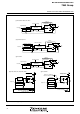
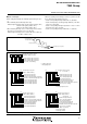
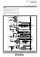
Fig. 20 Interrupt control
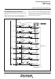
Fig. 21 Structure of interrupt-related registers
■Notes on interrupts
When setting the followings, the interrupt request bit may be set to
“1”.
•When switching external interrupt active edge
Related register: Interrupt edge selection register (address 3A16)
Timer X mode register (address 2716)
Timer Y mode register (address 2816)
•When switching interrupt sources of an interrupt vector address
where two or more interrupt sources are allocated
Related register: Interrupt source selection bit of A-D control reg-
ister (bit 6 of address 3416)
When not requiring for the interrupt occurrence synchronous with
these setting, take the following sequence.
➀Set the corresponding interrupt enable bit to “0” (disabled).
➁Set the interrupt edge select bit (polarity switch bit) or the inter-
rupt source selection bit.
➂Set the corresponding interrupt request bit to “0” after 1 or more
instructions have been executed.
➃Set the corresponding interrupt enable bit to “1” (enabled).
I
n
t
e
r
r
u
p
t
r
e
q
u
e
s
t
b
i
t
I
n
t
e
r
r
u
p
t
e
n
a
b
l
e
b
i
t
I
n
t
e
r
r
u
p
t
d
i
s
a
b
l
e
f
l
a
g
(
I
)
BRK instruction
Rese
t
Interrupt request acceptance
b
7
b
0
I
n
t
e
r
r
u
p
t
e
d
g
e
s
e
l
e
c
t
i
o
n
r
e
g
i
s
t
e
r
I
N
T
0
i
n
t
e
r
r
u
p
t
e
d
g
e
s
e
l
e
c
t
i
o
n
b
i
t
I
N
T
1
i
n
t
e
r
r
u
p
t
e
d
g
e
s
e
l
e
c
t
i
o
n
b
i
t
I
N
T
2
i
n
t
e
r
r
u
p
t
e
d
g
e
s
e
l
e
c
t
i
o
n
b
i
t
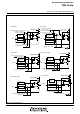
N
o
t
u
s
e
d
(
“
0
”
a
t
r
e
a
d
i
n
g
)
(INTEDGE
: a
dd
ress 003
A
16
)
I
n
t
e
r
r
u
p
t
r
e
q
u
e
s
t
r
e
g
i
s
t
e
r
1
I
N
T
0
i
n
t
e
r
r
u
p
t
r
e
q
u
e
s
t
b
i
t
I
N
T
1
i
n
t
e
r
r
u
p
t
r
e
q
u
e
s
t
b
i
t
S
e
r
i
a
l
I
/
O
1
r
e
c
e
i
v
e
i
n
t
e
r
r
u
p
t
r
e
q
u
e
s
t
b
i
t
S
e
r
i
a
l
I
/
O
1
t
r
a
n
s
m
i
t
i
n
t
e
r
r
u
p
t
r
e
q
u
e
s
t
b
i
t
T
i
m
e
r
X
i
n
t
e
r
r
u
p
t
r
e
q
u
e
s
t
b
i
t
T
i
m
e
r
Y
i
n
t
e
r
r
u
p
t
r
e
q
u
e
s
t
b
i
t
T
i
m
e
r
2
i
n
t
e
r
r
u
p
t
r
e
q
u
e
s
t
b
i
t
T
i
m
e
r
3
i
n
t
e
r
r
u
p
t
r
e
q
u
e
s
t
b
i
t
I
n
t
e
r
r
u
p
t
c
o
n
t
r
o
l
r
e
g
i
s
t
e
r
1
I
N
T
0
i
n
t
e
r
r
u
p
t
e
n
a
b
l
e
b
i
t
I
N
T
1
i
n
t
e
r
r
u
p
t
e
n
a
b
l
e
b
i
t
S
e
r
i
a
l
I
/
O
1
r
e
c
e
i
v
e
i
n
t
e
r
r
u
p
t
e
n
a
b
l
e
b
i
t
S
e
r
i
a
l
I
/
O
1
t
r
a
n
s
m
i
t
i
n
t
e
r
r
u
p
t
e
n
a
b
l
e
b
i
t
T
i
m
e
r
X
i
n
t
e
r
r
u
p
t
e
n
a
b
l
e
b
i
t
T
i
m
e
r
Y
i
n
t
e
r
r
u
p
t
e
n
a
b
l
e
b
i
t
T
i
m
e
r
2
i
n
t
e
r
r
u
p
t
e
n
a
b
l
e
b
i
t
T
i
m
e
r
3
i
n
t
e
r
r
u
p
t
e
n
a
b
l
e
b
i
t
0
:
N
o
i
n
t
e
r
r
u
p
t
r
e
q
u
e
s
t
i
s
s
u
e
d
1
:
I
n
t
e
r
r
u
p
t
r
e
q
u
e
s
t
i
s
s
u
e
d
(
I
R
E
Q
1
:
a
d
d
r
e
s
s
0
0
3
C
1
6
)
(
I
C
O
N
1
:
a
d
d
r
e
s
s
0
0
3
E
1
6
)
I
n
t
e
r
r
u
p
t
r
e
q
u
e
s
t
r
e
g
i
s
t
e
r
2
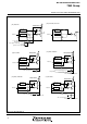
CNTR
0
i
nterrupt request
bi
t
CNTR
1
interrupt request bit
Timer 1 interrupt request bit
INT
2
interrupt request bit
Serial I/O2 interrupt request bit
Key input interrupt request bit
ADT/AD conversion interrupt request bit
Not used (“0” at reading)
(
I
R
E
Q
2
:
a
d
d
r
e
s
s
0
0
3
D
1
6
)
I
nterrupt contro
l
reg
i
ster 2
CNTR
0
i
nterrupt ena
bl
e
bi
t
CNTR
1
interrupt enable bit
Timer 1 interrupt enable bit
INT
2
interrupt enable bit
Serial I/O2 interrupt enable bit
Key input interrupt enable bit
ADT/AD conversion interrupt enable bit
Not used (“0” at reading)
(Write “0” to this bit)
0 :
I
nterrupts
di
sa
bl
e
d
1 : Interrupts enabled
(ICON
2 : a
dd
ress 003
F
16
)
0 :
F
a
lli
ng e
d
ge act
i
ve
1 : Rising edge active
b
7
b
0
b
7
b
0
b
7
b
0
b
7
b
0
0