
Specifications
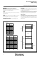

SINGLE-CHIP 8-BIT CMOS MICROCOMPUTER
MITSUBISHI MICROCOMPUTERS
7560 Group
16
I/O PORTS
Direction Registers
The I/O ports (ports P0, P1, P2, P4, P5, P6, P71–P77) have direc-
tion registers. Ports P16, P17, P4, P5, P6, and P71–P77 can be set
to input mode or output mode by each pin individually. P00–P07
and P10-P15 are respectively set to input mode or output mode in
a lump by bit 0 of the direction registers of ports P0 and P1 (see
Figure 13).
When “0” is set to the bit corresponding to a pin, that pin becomes
an input mode. When “1” is set to that bit, that pin becomes an
output mode.
If data is read from a port set to output mode, the value of the port
latch is read, not the value of the pin itself. A port set to input mode
is floating. If data is read from a port set to input mode, the value
of the pin itself is read. If a pin set to input mode is written to, only
the port latch is written to and the pin remains floating.
Port P3 Output Control Register
Bit 0 of the port P3 output control register (address 000716) en-
ables control of the output of ports P30–P37.
When the bit is set to “1”, the port output function is valid.
When resetting, bit 0 of the port P3 output control register is set to
“0” (the port output function is invalid) and pulled up.
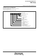
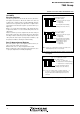
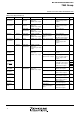
Fig. 13 Structure of port P0 direction register, port P1 direc-
tion register
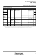
Fig. 14 Structure of port P3 output control register
P
orts
P
00 to
P
07
di
rect
i
on reg
i
ster
0 : Input mode
1 : Output mode
Not used (Undefined at reading)
(If writing to these bits, write “0”.)
P
ort
P
0
di
rect
i
on reg
i
ster
(P0D : address 0001
16)
b
7
b
0
N
ote:
I
n ports set to output mo
d
e, t
h
e pu
ll
-up contro
l
bi
t
b
ecomes
invalid and pull-up resistor is not connected.
P
orts
P
10 to
P
15
di
rect
i
on reg
i
ster
0 : Input mode
1 : Output mode
Not used (Undefined at reading)
(If writing to these bits, write “0”.)
Port P1
6 direction register
Port P1
7 direction register
0 : Input mode
1 : Output mode
P
ort
P
1
di
rect
i
on reg
i
ster
(P1D : address 0003
16)
b
7
b
0
P
orts
P
3
0
to
P
3
7
output contro
l
bi
t
0 : Output function is invalid (Pulled up)
1 : Output function is valid (No pull up)
Not used (Undefined at reading)
(If writing to these bits, write “0”.)
P
ort
P
3 output contro
l
reg
i
ster
(P3C : address 0007
16
)
b
7
b
0
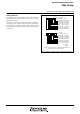
N
o
t
e
:
I
n
p
i
n
s
s
e
t
t
o
s
e
g
m
e
n
t
o
u
t
p
u
t
b
y
s
e
g
m
e
n
t
o
u
t
p
u
t
e
n
a
b
l
e
b
i
t
s
0
,
1
(
b
i
t
s
0
,
1
o
f
s
e
g
m
e
n
t
o
u
t
p
u
t
e
n
a
b
l
e
r
e
g
i
s
t
e
r
(
a
d
d
r
e
s
s
3
8
1
6
)
)
,
t
h
i
s
b
i
t
b
e
c
o
m
e
s
i
n
v
a
l
i
d
a
n
d
p
u
l
l
-
u
p
r
e
s
i
s
t
o
r
i
s
n
o
t
c
o
n
n
e
c
t
e
d
.