
Specifications

SINGLE-CHIP 8-BIT CMOS MICROCOMPUTER
MITSUBISHI MICROCOMPUTERS
7560 Group
15
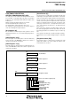
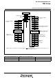
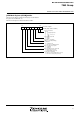
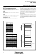
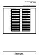
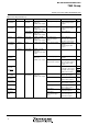
Fig. 12 Memory map of special function register (SFR)
0
0
2
01
6
0
0
2
11
6
0
0
2
21
6
0
0
2
31
6
0
0
2
41
6
002516
0
0
2
61
6
0
0
2
71
6
0
0
2
81
6
0
0
2
91
6
0
0
2
A
1
6
0
0
2
B
1
6
002
C
16
002
D
16
0
0
2
E
1
6
002
F
16
0
0
3
01
6
0
0
3
11
6
0
0
3
21
6
0
0
3
31
6
003416
0
0
3
51
6
003616
003716
003816
003916
003
A
16
0
0
3
B
1
6
003
C
16
003
D
16
0
0
3
E
1
6
003
F
16
0
0
0
01
6
0
0
0
11
6
0
0
0
21
6
0
0
0
31
6
0
0
0
41
6
000516
0
0
0
61
6
0
0
0
71
6
0
0
0
81
6
0
0
0
91
6
0
0
0
A
1
6
0
0
0
B
1
6
0
0
0
C
1
6
0
0
0
D
1
6
0
0
0
E
1
6
0
0
0
F
1
6
0
0
1
01
6
0
0
1
11
6
0
0
1
21
6
0
0
1
31
6
001416
0
0
1
51
6
001616
001716
001816
001916
001
A
16
001
B
16
001
C
16
001
D
16
0
0
1
E
1
6
0
0
1
F
1
6
P
o
r
t
P
0
r
e
g
i
s
t
e
r
(
P
0
)
P
o
r
t
P
1
r
e
g
i
s
t
e
r
(
P
1
)
P
ort
P
1
di
rect
i
on reg
i
ster
(P
1
D)
P
o
r
t
P
2
r
e
g
i
s
t
e
r
(
P
2
)
P
o
r
t
P
2
d
i
r
e
c
t
i
o
n
r
e
g
i
s
t
e
r
(
P
2
D
)
P
ort
P
3 reg
i
ster
(P
3
)
P
o
r
t
P
4
r
e
g
i
s
t
e
r
(
P
4
)
P
o
r
t
P
4
d
i
r
e
c
t
i
o
n
r
e
g
i
s
t
e
r
(
P
4
D
)
P
o
r
t
P
5
r
e
g
i
s
t
e
r
(
P
5
)
P
o
r
t
P
5
d
i
r
e
c
t
i
o
n
r
e
g
i
s
t
e
r
(
P
5
D
)
P
o
r
t
P
6
r
e
g
i
s
t
e
r
(
P
6
)
P
o
r
t
P
6
d
i
r
e
c
t
i
o
n
r
e
g
i
s
t
e
r
(
P
6
D
)
P
o
r
t
P
7
r
e
g
i
s
t
e
r
(
P
7
)
P
o
r
t
P
7
d
i
r
e
c
t
i
o
n
r
e
g
i
s
t
e
r
(
P
7
D
)
S
e
r
i
a
l
I
/
O
1
s
t
a
t
u
s
r
e
g
i
s
t
e
r
(
S
I
O
1
S
T
S
)
S
er
i
a
l
I
/
O
1 contro
l
reg
i
ster
(SIO
1
CON)
U
A
R
T
c
o
n
t
r
o
l
r
e
g
i
s
t
e
r
(
U
A
R
T
C
O
N
)
B
au
d
rate generator
(BRG)
I
n
t
e
r
r
u
p
t
c
o
n
t
r
o
l
r
e
g
i
s
t
e
r
2
(
I
C
O
N
2
)
T
i
m
e
r
3
r
e
g
i
s
t
e
r
(
T
3
)
T
i
m
e
r
X
m
o
d
e
r
e
g
i
s
t
e
r
(
T
X
M
)
I
n
t
e
r
r
u
p
t
e
d
g
e
s
e
l
e
c
t
i
o
n
r
e
g
i
s
t
e
r
(
I
N
T
E
D
G
E
)
CPU
mo
d
e reg
i
ster
(CPUM)
I
nterrupt request reg
i
ster 1
(IREQ
1
)
I
nterrupt request reg
i
ster 2
(IREQ
2
)
I
n
t
e
r
r
u
p
t
c
o
n
t
r
o
l
r
e
g
i
s
t
e
r
1
(
I
C
O
N
1
)
T
i
m
e
r
X
l
o
w
-
o
r
d
e
r
r
e
g
i
s
t
e
r
(
T
X
L
)
T
i
m
e
r
Y
l
o
w
-
o
r
d
e
r
r
e
g
i
s
t
e
r
(
T
Y
L
)
Ti
mer 1 reg
i
ster
(T
1
)
T
i
m
e
r
2
r
e
g
i
s
t
e
r
(
T
2
)
Ti
mer
X
hi
g
h
-or
d
er reg
i
ster
(TXH)
T
i
m
e
r
Y
h
i
g
h
-
o
r
d
e
r
r
e
g
i
s
t
e
r
(
T
Y
H
)
P
U
L
L
r
e
g
i
s
t
e
r
A
(
P
U
L
L
A
)
P
U
L
L
r
e
g
i
s
t
e
r
B
(
P
U
L
L
B
)
T
i
m
e
r
Y
m
o
d
e
r
e
g
i
s
t
e
r
(
T
Y
M
)
Ti
mer 123 mo
d
e reg
i
ster
(T
123
M)
T
O
U
T/φ
o
u
t
p
u
t
c
o
n
t
r
o
l
r
e
g
i
s
t
e
r
(
C
K
O
U
T
)
S
egment output ena
bl
e reg
i
ster
(SEG)
LCD
mo
d
e reg
i
ster
(LM)
A
-
D
c
o
n
t
r
o
l
r
e
g
i
s
t
e
r
(
A
D
C
O
N
)
A
-
D
convers
i
on
hi
g
h
-or
d
er
register (ADH)
T
ransm
i
t/
R
ece
i
ve
b
u
ff
er reg
i
ster
(TB
/
RB)
K
e
y
i
n
p
u
t
c
o
n
t
r
o
l
r
e
g
i
s
t
e
r
(
K
I
C
)
P
o
r
t
P
0
d
i
r
e
c
t
i
o
n
r
e
g
i
s
t
e
r
(
P
0
D
)
P
o
r
t
P
3
o
u
t
p
u
t
c
o
n
t
r
o
l
r
e
g
i
s
t
e
r
(
P
3
C
)
R
eserve
d
area
(N
ote
)
S
e
r
i
a
l
I
/
O
2
c
o
n
t
r
o
l
r
e
g
i
s
t
e
r
(
S
I
O
2
C
O
N
)
S
e
r
i
a
l
I
/
O
2
r
e
g
i
s
t
e
r
(
S
I
O
2
)
P
W
M
c
o
n
t
r
o
l
r
e
g
i
s
t
e
r
(
P
W
M
C
O
N
)
PWM
presca
l
er
(PREPWM)
PWM
reg
i
ster
(PWM)
R
eserve
d
area
(N
ote
)
R
eserve
d
area
(N
ote
)
R
e
s
e
r
v
e
d
a
r
e
a
(
N
o
t
e
)
R
eserve
d
area
(N
ote
)
D
-
A
1
c
o
n
v
e
r
s
i
o
n
r
e
g
i
s
t
e
r
(
D
A
1
)
D
-
A
2 convers
i
on reg
i
ster
(DA
2
)
D
-
A
contro
l
reg
i
ster
(DACON)
W
a
t
c
h
d
o
g
t
i
m
e
r
c
o
n
t
r
o
l
r
e
g
i
s
t
e
r
(
W
D
T
C
O
N
)
N
ote:
D
o not wr
i
te to t
h
e a
dd
resses o
f
reserve
d
area.
A
-
D
c
o
n
v
e
r
s
i
o
n
l
o
w
-
o
r
d
e
r
r
e
g
i
s
t
e
r
(
A
D
L
)