
Datasheet


©2008. Renesas Technology Corp., All rights reserved.
9
Rev.1.00 Date: Aug.04.08
REJ99B2001-0100
According to the differences in the specifications shown in P.6, the following notes are suggested. Please also refer to P.6.
1. Program Memory
Depending on the memory type, program/erase specifications as well as applicable programmers and adaptors differ.
Confirm the programmer applicable for your product.
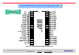
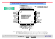
2. Packages
- The WG-package product is available only in the 3804L Group.
- In the 3804L Group, the FP package product is not available, but the thin KP package product is available for 0.8 mm-pitch.
As a 0.8 mm-pitch, the KP package has better excellence in thinness, heat radiation, and stress characteristics than FP package.
Confirm the mounting pad design standards of FP package and KP package on Renesas Surface Mount Package User's
Manual (Document No.: REJ11K0001)
3. Operating Power Source Voltage
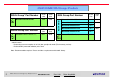
- The operating power source voltage for the 3804 Group Mask ROM version and the 3804H/3804L Groups ranges from 2.7 to 5.5V.
It ranges from 4.0 to 5.5 V for 3804 Group Flash memory version. Confirm the operating power source voltage for your product.
4. Flash Memory ID Code and ROM Code Protect
In the 3804H/3804L Groups Flash memory version, ID codes are assigned to addresses FFD4 to FFDA16, and ROM code protect is
assigned to address FFDB16. Please note that these addresses are included in the user ROM area. The data of these addresses
must be set to programming data before programming.
5. Flash Memory Control Registers
- In the 3804H/3804L Group Flash memory version, Flash Memory control registers 0 to 2 are assigned to addresses 0FE0 to 0FE216.
- In the 3804 Group Flash memory version, Flash Memory control register is assigned to address 0FFE16 and Flash command
register is assigned to address 0FFF16.
- In the Mask ROM versions, nothing is allocated to these addresses, so writing can be performed to them. When read, their values
are undefined.
Replacement Notes (1)
Replacement Notes (1)