
Datasheet


©2008. Renesas Technology Corp., All rights reserved.
12
Rev.1.00 Date: Aug.04.08
REJ99B2001-0100
Vcc
SDA (P44/RXD1)
SCLK (P46/SCLK1)
OE (P37/SRDY3)
BUSY (P47/SRDY1 /CNTR2)
TXD (P45/TXD1)
VPP (CNVSS)
RESET(RESET)
Vss
M38049FF
(Standard serial I/O Mode)
T_VDD
T_TXD
T_RXD
T_SCLK
T_PGM/OE/MD
T_BUSY
T_VPP
T_RESET
USER RST
GND
57
15
13
49
12
14
18
19
24
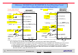
Reference: M38049FF and M38049FFH (L) Serial Rewriting Circuit
when Using a Suisei Electronics System Serial Unit
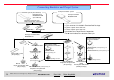
Reference: M38049FF and M38049FFH (L) Serial Rewriting Circuit
when Using a Suisei Electronics System Serial Unit
The pin number indicates
the flat package version.
Note: T_VPP is not needed.
N.C.
XIN XOUT
Perform the same pin processing as in single chip mode.
*3
*1
M38049FFH
M38049FFL
(Standard serial I/O Mode 1)
Vcc
RXD (P44/RXD1)
SCLK (P46/SCLK1)
BUSY (P47/SRDY1/CNTR2)
TXD (P45/TXD1)
CNVSS
RESET(RESET)
Vss
57
15
13
12
14
18
19
24
T_VDD
T_TXD
T_SCLK
T_BUSY
T_RXD
T_PGM/OE/MD
T_RESET
USER RST
GND
XIN XOUT
Perform the same pin processing as in single chip mode.
*2
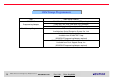
Differences
Note:
z As programming specifications differ for each product, specify the part number before programming.
z As the MCU programming pins are common, writing can be performed on the same board in the QzROM/Flash memory versions.
*1: For the standard version, connect both the serial unit’s T_TXD and T_RXD to SDA (RxD pin), and leave TxD pin open.
*2: Supply the power source voltage (Vcc) from the user so that it will meet the Vcc of the output buffer used on the programmer.
*3: The VDD power source is supplied from the programmer. When the user power consumption is high (20 mA or more for
other than the MCU), supply the VDD from the user.