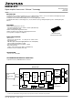
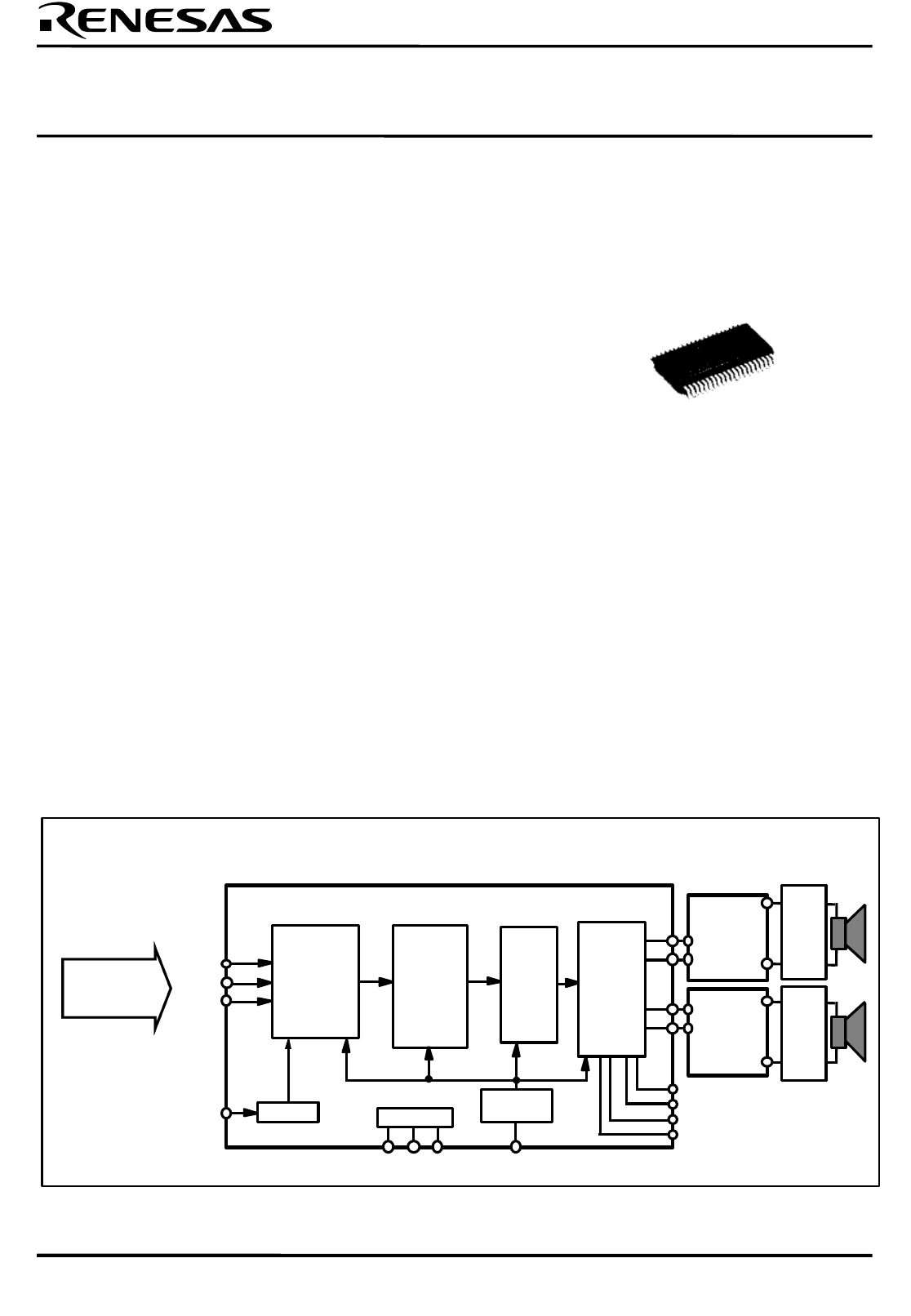
M65881AFP REJ03F0004-0100Z Rev.1.00 2003.05.08 Digital Amplifier Processor of S-Master* Technology DESCRIPTION The M65881AFP is a S-Master technique processor for digital amplifier enable to convert from multi liner-PCM digital input signal to high precise switching-pulse digital output without analog processing. The M65881AFP has built-in 24bit sampling rate converter and digital-gain-controller. The M65881AFP enables to realize high precise ( X`tal oscillation accuracy.
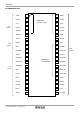
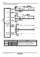
M65881AFP PIN CONFIGURATION 3.3V system 1.8V system 3.
Rev.1.00 2003.05.
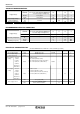
M65881AFP ABSOLUTE MAXIMUM RATINGS Parameter Symbol Condition Min. Typ. Max Unit PWMVdd 3.3V system (XVdd, XOVdd, PWM Output for Power Stage & Headphone) -0.3 – 3.8 V BFVdd DVdd Vi Pd Tstg 3.3V system 1.8V system -0.3 -0.3 -0.3 3.8 2.5 Vdd+0.3 -40 – – – 350 – 125 V V V mW ºC Supply Voltage Input Voltage Range Power Dissipation Storage Temperature Ta=75ºC RECOMMENDED OPERATING CONDITIONS Parameter Supply Voltage Symbol Condition Min. Typ. Max Unit PWMVdd 3.
M65881AFP CHARACTERISTICS EVALUATION CIRCUIT OUTL1 2 + + - + GND OUTL2 4 + - OUTR2 39 + OUTR1 41 + - LRCK 16 BCK 17 + - + - GND DATA 18 M65881AFP HPOUTL1 33 + HPOUTL2 31 Power Supply GND HPOUTR2 27 HPOUTR1 29 Reference characteristic S/N 102dB(typ) Output for Power Stage THD+N 0.002%(typ) S/N 100dB(typ) Output for Headphone THD+N 0.006%(typ) Rev.1.00 2003.05.08 page 5 of 23 + - Conditions • Input :1kHz 0dB Full scale sine wave • FS :Primary clock 44.
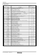
M65881AFP PIN DESCRIPTION Pin No. Name 1 2 3 4 5 6 7 8 9 10 11 12 13 14 15 16 17 18 19 20 21 22 23 24 25 26 27 28 29 30 31 32 33 34 35 36 37 38 39 40 41 42 VddL OUTL1 VssL OUTL2 XOVdd XfsoOUT XOVss DVdd DVss MCKSEL SCDT SCSHIFT SCLATCH NSPMUTE INIT LRCK BCK DATA BFVdd BFVss XfsiIN FsoCKO FsoI SFLAG TEST2 TEST1 HPOUTR2 HPVssR HPOUTR1 HPVddR HPOUTL2 HPVssL HPOUTL1 HPVddL XVss XfsoIN XVdd VssLR OUTR2 VssR OUTR1 VddR Rev.1.00 2003.05.08 Description I/O Power Supply for Lch PWM Power Stage (3.
M65881AFP EXPLANATION OF OPERATION 1. DATA,BCK,LRCK DATA,BCK, and LRCK are input pins for Digital Audio Signal of CD, MD, DVD etc.. Input formats are supported by 4 ways, and are set by Serial Control, "System1 Mode, bit3 and bit4". Input data length are selectable in a case of "MSB First Right Justified" (Serial Control "System1 Mode,bit5 and bit6"). •Input formats are shown in following figures.
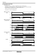
M65881AFP 2. SCDT, SCSHIFT, SCLATCH SCDT, SCSHIFT and SCLATCH are input pins for setting M65881AFP's operation. Input format of SCDT, SCSHIFT and SCLATCH is shown below. Input Format of SCDT, SCSHIFT and SCLATCH 24 SCDT 20 15 bit1 10 5 1 SCSHIFT SCLATCH • Mode Setting The operating mode are classified in four and assigned by bit1 and bit2. These four functions are shown below. ( bit1 and bit2 )= ( "L" and "L" ) Gain control mode: Gain control.
M65881AFP 5. FsoCKO FsoCKO is clock output pin of 1fso frequency. The output is divided-clock of XfsoIN, and frequency is free-running at power on. FsoCKO pin's clock is utilized for a synchronization in case that have used plural M65881AFP, take a synchronization between M65881AFP and other external devices. Refer to the following Chapter 6. in detail. 6. FsoI, SFLAG M65881AFP synchronizes in clock input from the external source devices.
M65881AFP 7. OUTL1, OUTL2, OUTR1, OUTR2 OUTL1, OUTL2, OUTR1 and OUTR2 are pulse output modulated ∆Σ output to PWM signal. These pins are connected to external Power Driver ICs.The PWM output can be selected PWM Output Format 1, 2, 3 and 4 by serial control data(System1 mode, bit22,23 ). PWM Output Form1 : General Modulation PWM Output Form2 : Symmetrical Modulation PWM Output Form3 : Modulation returned with time domain. ( The rise and fall edge of Lch and Rch in a term are reverse.
M65881AFP 8. HPOUTL1, HPOUTL2, HPOUTR1, HPOUTR2 HPOUTL1, HPOUTL2, HPOUTR1 and HPOUTR2 are output pins for Headphone output. PWM output modulated ∆Σ output data to pulse width. The Phase of PWM Output for Power Stage and PWM Output for Headphone. The output for Headphone is reverse phase as output for Power. Moreover, it is possible to set L1 and R1 output same phase by serial control the system 1 mode, bit24= "H"( PWMHP ).
M65881AFP 13. Power sequences System power-on sequencing * Refer to following figure. Power(Vddxxx, HPVddxxx, XVdd, XOVdd, DVdd, BFVdd) Power OFF Power ON Master clock (XfsoIN,XfsiIN) X INIT X SCDT X SCSHIFT X SCLATCH X Over 5msec(*1) Over 0sec(*2) Over 2/fso(*3) *1 After a power supply and Master clock become to stable, INIT pin must be "L" over 5msec. *2 Data transfer is possible right after INIT release.
M65881AFP SERIAL CONTROL 1.
M65881AFP The index and Mantissa part of Gain Data (bit12-bit24 :GAIN0-GAIN12) The gain value is set from bit12-bit24. Index part: bit12(MSB) to bit16(LSB) Mantissa part: bit17(MSB) to bit24(LSB) The gain data is assigned 13bits, composed of Index part 5bits and of Mantissa part 8bits. The range of Index parts is following statements. Index part: 10100b(16.0) to 10000b(1.0) to 00000b(2-16) The range of Mantissa parts is following statements.
M65881AFP • Soft Mute The Soft Mute function is executed by setting of Gain Data as 00000/00000000b (" / " means dividing point between index part and mantissa part). The release from Soft Mute Function must be executed by setting the gain data before soft mute. The Soft mute Function and release from there don't have linear curve but have characteristics of approximate exponential curve. Output amplitude 16.0 0.
M65881AFP 2. System1 Mode bit 1 2 3 4 5 6 7 8 9 10 11 12 13 14 15 16 17 18 19 20 21 22 23 24 Flag name MODE1 MODE2 IFMT0 IFMT1 IBIT0 IBIT1 ISF0 ISF1 EMPFS1 EMPFS2 DF1IMUTE DF2IMUTE Function Explanation Mode Setting 1 Mode Setting 2 No setting bits means "Don't care".
M65881AFP Fs Selection for De-emphasis filter (De-emphasis is "ON" except for bit9="L" and bit10="L". (bit9, bit10) : ("L", "L") …De-emphasis Filter off except ("L", "L") … De-emphasis Filter on (Setting fsi) Zero Mute at DATA input ( bit11: DF1IMUTE ) "L" … Mute release "H" … Mute The input data from DATA pin is muted in this setting. Zero Mute at Sampling Rate Converter Input (bit12: DF2IMUTE) "L" … Mute release "H" … Mute DF2IMUTE is muting control of sampling rate converter input data.
M65881AFP 3. System2 Mode bit 1 2 3 4 5 6 7 8 9 10 11 12 13 14 15 16 17 18 19 20 21 22 23 24 No setting bits means "Don't care".
M65881AFP Flag to " Enable " of Asynchronous Detection for secondary block ( bit8: ASYNCEN2) ASYNCEN2 (bit8 ) controls " Enable" and " Disable" for secondary asynchronous detector. "L“ … "disable" "H" … "enable“ Under condition of ASYNCEN2="L", secondary side asynchronous detection is in-effective under asynchronous position, whether Fsol Clock is not inputted, there by M65881AFP does not operate function for instance mute operation.
M65881AFP AC CHARACTERISTICS (Ta=25ºC, PWMVdd=3.3V, DVdd=1.8V) Item XfsoIN Duty Ratio Symbol duty(XfsoIN) XfsiIN Duty Ratio duty(XfsiIN) SCSHIFT Pulse time SCDT Setup time SCDT Hold time SCLATCH Pulse Width SCLATCH Setup Time SCLATCH Hold time BCK Pulse Width DATA Setup Time DATA Hold time LRCK Setup time LRCK Hold time Condition 512fsi 256fsi tw (SCSHIFT) tsu (SCDT) th (SCDT) tw (SCLATCH) tsu (SCLATCH) th (SCLATCH) tw (BCK) tsu (DATA) th (DATA) tsu (LRCK) th (LRCK) Min.
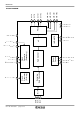
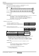
M65881AFP APPLICATION EXAMPLE DSP LRCK BCK DATA XfsiIN (Primary Clock) MCKSEL XFSOIN (Secondary Clock) XFSOOUT FsoCKO FsoI MCU Secondary Clock Select L:1024Fso H:512Fso SCDT SCSHIFT SCLATCH OUTL1 OUTL2 Oscillator Secondary Clock output Secondary synchronized clock (For Multi channel ) Power Driver M65881AFP Initialize Control INIT Mute Control NSPMUTE OUTR1 OUTR2 Input Mode Select1 Input Mode Select2 HPOUTL1 MODE1 MODE2 T E S T 1 T E S T 2 S F L A G HPOUTL2 HPOUTR1 HPOUTR2 Flag Outpu
HE page 22 of 23 G 1 42 Z1 e EIAJ Package Code SSOP42-P-450-0.80 E z y Detail G D JEDEC Code – MMP b 21 22 Weight(g) – Detail F A2 Lead Material Cu Alloy+42 Alloy L1 Rev.1.00 2003.05.08 A c A1 F L A A1 A2 b c D E e HE L L1 z Z1 y Symbol e1 b2 e1 I2 b2 Dimension in Millimeters Min Nom Max 2.4 – – – 0.05 – – 2.0 – 0.4 0.3 0.25 0.2 0.15 0.13 17.7 17.5 17.3 8.6 8.4 8.2 – 0.8 – 12.23 11.93 11.63 0.7 0.5 0.3 – 1.765 – – 0.75 – – – 0.9 0.15 – – 0° – 10° – 0.5 – – 11.43 – – 1.
M65881AFP Sales Strategic Planning Div. Nippon Bldg., 2-6-2, Ohte-machi, Chiyoda-ku, Tokyo 100-0004, Japan Keep safety first in your circuit designs! 1. Renesas Technology Corporation puts the maximum effort into making semiconductor products better and more reliable, but there is always the possibility that trouble may occur with them. Trouble with semiconductors may lead to personal injury, fire or property damage.