M61323SP/FP Wide Frequency Band Analog Switch REJ03F0201-0201 Rev.2.01 Mar 31, 2008 Description The M61323SP/FP is a semiconductor integrated circuit for the RGBHV interface. The device features switching signals input from two types of image sources and outputting the signals to the CRT display, etc. Synchronous signals, meeting a frequency band of 10 kHz to 200 kHz, are output at TTL.
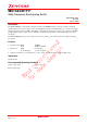
M61323SP/FP Block Diagram M61323SP Output (G) Output (R) GND VCC (R) 32 31 30 29 VCC (R) 28 27 26 25 VCC (G) 2 Input1 (R) VCC (R) B 4 21 20 6 Input1 (G) Sync-Sep. G 7 8 Input1 (B) VCC (B) 19 18 17 9 10 Input1 (V) Input1 (H) V H POWER SAVE SW GND 5 VCC (G) 22 VCC VCC (B) 3 23 GND VCC Sync-Sep. INPUT 24 Output (V) Output (H) VCC (B) G VCC (R) GND VCC (B) VCC (G) R 1 GND VCC (G) Sync-Sep.
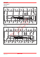
M61323SP/FP Pin Arrangement M61323SP M61323FP VCC1 (R) 1 36 NC 31 Output (R) Input1 (R) 2 35 VCC2 (R) 3 30 GND2 (R) VCC1 (G) 3 34 Output (R) Input1 (G) 4 29 VCC2 (G) Input1 (G) 4 33 GND2 (R) VCC1 (B) 5 28 Output (G) VCC1 (B) 5 32 VCC2 (G) Input1 (B) 6 27 GND2 (G) Input1 (B) 6 31 Output (G) 7 26 Input1 (H) 7 30 GND2 (G) Input1 (V) VCC1 (R) 1 32 VCC2 (R) Input1 (R) 2 VCC1 (G) Input1 (H) VCC2 (B) 8 25 Output (B) 8 29 GND1 9 24 GND2 (B) GND1 9 28 Output (B)
M61323SP/FP Absolute Maximum Ratings (Ta = 25°C) Item Symbol Ratings 7.0 Unit V Supply voltage VCC Power dissipation Operating temperature Storage temperature Electrostatic discharge Recommended supply voltage Pd Topr Tstg Surge Vopr 1603 (SP), 1068 (FP) −20 to +85 (SP), −20 to +75 (FP) −40 to +150 ±200 5.0 mW °C °C V V Recommended supply voltage range Vopr' 4.75 to 5.25 V Electrical Characteristics (M61323SP VCC = 5.
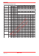
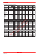
M61323SP/FP Electrical Characteristics (cont.) Limits Item Freq. characteristic1 (100 MHz) Test Point SW2 SW4 Symbol Min. Typ. Max. Unit (s) Rin1 Gin1 dB −1 0 1 abb bab 31 FC1 Relative Freq.characteristic1 (100 MHz) ∆FC1 −1 0 1 dB Freq.characteristic2 (100 MHz) FC2 −1 0 1 dB Relative Freq.characteristic2 (100 MHz) Freq.characteristic3 (250 MHz) ∆FC2 −1 0 1 dB FC3 −3 dB Freq.characteristic4 (250 MHz) FC4 −3 dB Crosstalk between two inputs1 (10 MHz) C.T.I.
M61323SP/FP Electrical Characteristics (cont.) Test Input SW Point SW2 SW4 SW6 SW7 SW8 SW10 SW12 SW14 SW15 SW16 SW22 SW11 SW13 Symbol Min. Typ. Max. Unit (s) Rin1 Gin1 Bin1 Hin1 Vin1 Rin2 Gin2 Bin2 Hin2 Vin2 Sync P.sav Switch Limits Item HV SW High level output voltage1 Vdch1 3.8 4.2 V 18 19 b b b a SG8 a SG8 b b b b b b a 3V b High level output voltage2 Vdch2 3.8 4.2 V 18 19 b b b b b b b b a SG8 a SG8 b a 3V a 3V Low level output voltage1 Vdcl1 0.2 0.
M61323SP/FP Electrical Characteristics Test Method (M61323SP) Circuit Current 1 No signal. Measure the total circuit current as ICC when supplying 3 VDC to pin 11. Circuit Current 2 No signal. Measure the total circuit current as ICCSTBY when pin 11 connected to GND. Output DC Voltage 1, 2 Set SW13 to GND (or OPEN), measure the DC voltage of TP31 (TP28, TP25) when there is no signal input. The DC voltage is as vdc1 (vdc2). Output DC Voltage 3, 4 Measure the DC voltage TP23 same as "Output DC voltage 1, 2".
M61323SP/FP Freq. Characteristic 3, 4 Measure the FC3, FC4 when SG5 of input signal. (For reference) Crosstalk between Two Inputs 1, 2 1. 2. 3. 4. The conditions is as table. This measurement shall use active probe. Set SW13 to GND, input SG3 to pin 2 only. Read the output amplitude of TP31. The value is as VOR3. Then set SW13 to OPEN, read the output amplitude of TP31. The value is as VOR3'. Crosstalk between two inputs 1 C.T.I.1 is C.T.I.1 = 20log 5. 6. 7. 8.
M61323SP/FP Pulse Characteristic 1, 2 1. 2. 3. 4. The conditions is as table (SG5 amplitude 0.7 VP-P). Set SW13 to GND (or OPEN). Measure rising Tri and falling Tfi for 10% to 90% of the input pulse with active probe. Next, measure rising Tro and falling Tfo for 10% to 90% of the output pulse with active probe.
M61323SP/FP Sync Input Minimum Voltage Gradually decreasing the amplitude of SG7 in pin 22, measure the amplitude of SG7 when the Sync-Sep output signal turn off. The value is as SYrv. Sync Output High Level Voltage/Sync Output Low Level Voltage Input SG7 to pin 22, read the output high level and low voltage of TP21. The value is as SYVH, SYVL. Sync Output Rising Time/Sync Output Falling Time 1. The conditions is as table. (SG7 amplitude 0.3 VP-P) This measurement shall use active probe.
M61323SP/FP Input Signal SG No. SG1 Signals Sine wave (f = 60 kHz, 0.7 VP-P (Amplitude variable) ) 0.7 VP-P (variable) SG2 SG3 SG4 SG5 SG6 Sine wave (f = 1 MHz, 0.7 VP-P (Amplitude variable) ) Sine wave (f = 10 MHz, 0.7 VP-P (Amplitude variable) ) Sine wave (f = 100 MHz, 0.7 VP-P (Amplitude variable) ) Sine wave (f = 250 MHz, 0.7 VP-P (Amplitude variable) ) DUTY 80% fH = 60 kHz 0.7 VP-P 0.7 VP-P SG7 Sync (fH = 60 kHz) Amplitude variable (Typ. = 0.3 VP-P) 4.
M61323SP/FP Test Circuit (M61323SP) TP23 SG SS b 0.01 µ a VCCC 5 V SW22 29 G-SW VCC 0.01 µ 24 23 4 TP19 TP18 22 21 20 6 7 8 9 10 0.01 µ 11 12 13 TP11 TP13 SW11 SW13 SW7 SW8 a SW2 a SW4 b a ba 17 14 15 16 a SG RGB + 75 + 75 + SW15 SW16 75 b a SW6 b 18 a b c open 47 µ 47 µ 75 0.01 µ 75 19 + 47 µ 75 0.01 µ + 47 µ 0.01 µ a b c open + 47 µ ECO-SW 5 0.01 µ 0.01 µ a A VCC 47 µ 0.01 µ 25 0.
M61323SP/FP Application Example (M61323SP) OUTPUT VCC 5V + ROUT GOUT BOUT G Buffer OUT Sync SEP OUT 47 µ Hout 47 µ 47 µ 47 µ + 0.01 µ + 0.01 µ + 0.01 µ 0.01 µ Vout 1µ + 47 µ + 30 29 VCC 28 27 26 VCC R VCC (5 V) 75 20 5 19 18 H 75 POWER SAVE VCC (H-SW, V-SW, G-Buffer, Sync-SEP) Power save SW 6 7 8 9 10 11 12 13 14 15 16 75 75 + 75 + + 47 µ + 0.01 µ 0 to 0.8 V : INPUT1 2.0 to 5.0 V: INPUT2 47 µ + 17 0.01 µ V 0.01 µ 0.
M61323SP/FP Pin Description (M61323SP) pin No. 1 3 5 20 26 29 32 2 4 6 10 12 14 Name VCC (R) VCC (G) VCC (B) VCC (H, V, Sync-Sep.) VCC (ROUT) VCC (GOUT) VCC (BOUT) Input1 (R) Input1 (G) Input1 (B) Input2 (R) Input2 (G) Input2 (B) DC Voltage (V) 5.0 Peripheral Circuit Function 5.0 Input signal with low impedance 2.3 750 3V 643 2.48 V 2.2 mA 7 8 15 16 Input1 (H) Input1 (V) Input2 (H) Input2 (V) Input pulse between 3 V and 5 V 3 to 5 V 500 0 to 0.
M61323SP/FP Pin Description (M61323SP) (cont.) pin No. 11 Name PwrSave-SW DC Voltage (V) 2.5 Peripheral Circuit Function Do not apply more 5 V DC voltage 30 k 15 k 25 k 2.0 V 10 k 20 k 13 CONT-SW 20 k 25 k 20 k 2.4 Do not apply more 5 V DC voltage 26 k 15 k 5k 2.4 V 24 k 18 19 Vout Hout 7.3 k 20 k 100 15 k 15 k REJ03F0201-0201 Rev.2.
M61323SP/FP Pin Description (M61323SP) (cont.) pin No. 21 Name Sync sep OUT DC Voltage (V) Peripheral Circuit Function 15 k 100 15 k 15 k 22 Sync sep IN Connect a capacitance between the pin and GND when not use SYNC-SEP 10 k 10 k 2k Vth CLAMPref 23 G Buffer OUT 5k 5k 2k 25 28 31 Video OUT (B) Video OUT (G) Video OUT (R) 1.5 32, 29, 26 pin 50 31, 28, 25 pin 30, 27, 24 pin REJ03F0201-0201 Rev.2.
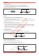
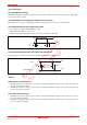
M61323SP/FP Note How to Use This IC (M61323SP) 1. 2. 3. 4. R, G, B input signal is 0.7 VP-P of standard video signal. H, V input is 5.0 V TTL type. Input signal with sufficient low impedance to input terminal. The terminal of R, G, B output pin are shown as figure 1. When resistance is connected between the pin 31 (28, 25) and GND, ICC will be increase. 5. Switch (pin 13) can be changed by supplying some voltage as figure 2. 0 to 0.5 V: INPUT1 2.5 to 5 V: INPUT2 Do not apply VCC or more DC voltage. 6.
M61323SP/FP Cautions for Manufacturing Boards Built-in wide band preamplifier may cause oscillation due to the wiring shape on the board. Be careful for the following points. • VCC shall use a stable power supply. (Individual VCC should use an independent power supply.) • GND should be as wide as possible. Basically, solid earth should be used. Make the load capacitance of output pins as small as possible. • Also ground the hold capacitance to stable GND, which is as near to the pin as possible.
M61323SP/FP Package Dimensions RENESAS Code PRDP0032BA-A Previous Code 32P4B MASS[Typ.] 2.2g 17 1 16 *1 E 32 e1 JEITA Package Code P-SDIP32-8.9x28-1.78 c D Reference Symbol e1 D E A A1 A2 bp b2 b3 c L A1 A A2 *2 NOTE) 1. DIMENSIONS "*1" AND "*2" DO NOT INCLUDE MOLD FLASH. 2. DIMENSION "*3" DOES NOT INCLUDE TRIM OFFSET. SEATING PLANE *3 b 3 e bp *3 b2 e L JEITA Package Code P-SSOP36-8.4x15-0.80 RENESAS Code PRSP0036GA-B Previous Code 36P2R-D Min Nom Max 9.86 10.16 10.46 27.
Sales Strategic Planning Div. Nippon Bldg., 2-6-2, Ohte-machi, Chiyoda-ku, Tokyo 100-0004, Japan Notes: 1. This document is provided for reference purposes only so that Renesas customers may select the appropriate Renesas products for their use.