REJ10J1564-0104 SH7285 CPU Board 32 M3A-HS85 User's Manual Renesas 32-Bit RISC Microcomputers SuperH RISCengine Family / SH7285 Group TM Rev. 1.
Notes regarding these materials 1. This document is provided for reference purposes only so that Renesas customers may select the appropriate Renesas products for their use. Renesas neither makes warranties or representations with respect to the accuracy or completeness of the information contained in this document nor grants any license to any intellectual property rights or any other rights of Renesas or any third party with respect to the information in this document. 2.
Table of Contents Chapter1 Overview .............................................................................................................................. 1-1 1.1 Overview .................................................................................................................................................................... 1-2 1.2 Configuration .................................................................................................................................................
3.2.4 Serial Port Select Jumper (JP7, JP8) .............................................................................................................. 3-22 3.2.5 Switch and LED Functions .............................................................................................................................. 3-23 3.2.6 Jumper Switch Setting when Using Development Tool ................................................................................... 3-25 3.3 Board Dimensions of M3A-HS85.............
Chapter1Overview Chapter1 Overview 1-1
Overview 1 1.1 Overview 1.1 Overview The M3A-HS85 is the CPU board designed for users to evaluate the functionality and performance of the SH7285 group of Renesas Technology original microcomputer, as well as develop and evaluate the application software for this group of microcomputers.
Overview 1 1.3 External Specifications 1.3 External Specifications Table 1.3.1 lists the external specifications of M3A-HS85. Table 1.3.1 External Specifications of M3A-HS85 No. Item Content SH7285 1 CPU z Input(XIN) Clock: 12.5 MHz z CPU Clock: Maximum 100 MHz z Bus Clock: Maximum 50 MHz z On-chip memory • Flash Memory: 768 KB • RAM: 32 KB z SRAM: 2-Mbyte (16-bit bus width x 1 pc.) (Not mounted) *Can be mounted only when SH7285 is used in 3.3V.
Overview 1 1.4 External View 1.4 External View Figure 1.4.1 shows the external view of M3A-HS85. Figure 1.4.1 External View of M3A-HS85 Rev.1.04 2008.07.
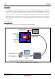
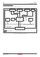
Overview 1 1.5 M3A-HS85 Block Diagram 1.5 M3A-HS85 Block Diagram Figure 1.5.1 shows the system block diagram of M3A-HS85. H-UDI connector (36-pin) Serial Port Connector H-UDI connector (14-pin) USB Connector H-UDI AUD SCI0 USB EEPROM (128 k-bit) SRAM 2 MB I2C SH7285 (100 MHz) * 16 USBXIN (48 MHz) XIN (12.5 MHz) 16 SDRAM 16 MB * 16 External bus: Maximum 50 MHz SH7285 CPU Board M3A-HS85 16 Extension Connectors : It is not mounted. * : It can be mounted only when SH7285 is used in 3.3V.
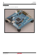
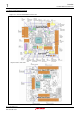
Overview 1 1.6 M3A-HS85 Board Overview 1.6 M3A-HS85 Board Overview Figure 1.6.1 shows the M3A-HS85 board overview. Figure 1.6.1 M3A-HS85 Board Overview Rev.1.04 2008.07.
Overview 1 1.6 M3A-HS85 Board Overview Table 1.6.1 lists the main components mounted on the M3A-HS85. Table 1.6.
Overview 1 1.7 M3A-HS85 Memory Mapping 1.7 M3A-HS85 Memory Mapping Figure 1.7.1, Figure 1.7.2, and Figure 1.7.3 show the memory mapping examples of SH7285 in the M3A-HS85.
Overview 1 1.
Overview 1 1.
Overview 1 1.8 Absolute Maximum Ratings 1.8 Absolute Maximum Ratings Table 1.8.1 lists the absolute maximum rating of M3A-HS85. Table 1.8.1 Absolute Maximum Ratings of M3A-HS85 Symbol Parameter Rated Value 5VCC 5V System Power Supply Voltage -0.3V to 6.0V Relative to VSS 3VCC 3.3V -0.3V to 4.6V Relative to VSS 0°C to 50°C No dewdrops allowed. System Power Supply Remarks Voltage Topr Operating Ambient Temperature Use in corrosive gas environment prohibited.
Overview 1 1.8 Absolute Maximum Ratings *This is a blank page* Rev.1.04 2008.07.
Chapter2Functional Overview Chapter2 Functional Overview 2-1
Functional Overview 2 2.1 Functional Overview 2.1 Functional Overview The M3A-HS85 is the SH7285 CPU board that has the functions listed in Table 2.1.1. Table 2.1.1 lists the functional modules of M3A-HS85. Table 2.1.1 Functional Modules of M3A-HS85 Section 2.2 Function CPU Content SH7285 • Input(XIN) Clock: 12.5 MHz • CPU Clock: Maximum 100 MHz • Bus Clock: Maximum 50 MHz • On-Chip Memory - Flash Memory: 768 kBytes - RAM: 32 kBytes 2.3 Memory • SRAM : 2-Mbyte (16-bit bus width x 1pc.
Functional Overview 2 2.2 CPU 2.2 CPU The M3A-HS85 contains the 32-bit RISC microcomputer SH7285 that operates with a maximum 100MHz of CPU clock frequency. The SH7285 includes 768-Kbyte flash memory, and 32-Kbyte RAM, making it useful in a wide range of applications from data processing to equipment control. The M3A-HS85 can be operated with a maximum 100MHz of CPU clock frequency (external bus maximum 50 MHz) using a 12.5 MHz input clock. Figure 2.2.1 shows the SH7285 block diagram in the M3A-HS85.
Functional Overview 2 2.3 Memory 2.3 Memory 2.3.1 SH7285 On-Chip Memory The SH7285 includes a 768-Kbytes flash memory and 32-Kbytes RAM. 2.3.2 SRAM Two Mbytes of SRAM can be mounted on the M3A-HS85 (Not mounted). In the M3A-HS85 specification, 3.3V power is supplied to SRAM so that SH7285 should be used in 3.3V when SRAM is mounted (CPU power supply switch jumper (JP1) should be set to “2-3”). SRAM is controlled by the bus state controller built into SH7285.
Functional Overview 2 2.3.3 SDRAM 2.3.3 SDRAM The M3A-HS85 can mount 16Mbytes of SDRAM (Not mounted). In the M3A-HS85 specification, 3.3V power is supplied to SDRAM so that SH7285 should be used in 3.3V when SDRAM is mounted (CPU power supply switch jumper (JP1) should be set to “2-3”). The SDRAM is controlled by the bus state controller built into SH7285. Table 2.3.2 lists the SDRAM specifications. Figure 2.3.2 shows the block diagram for the connection between SH7285 and SDRAM. Table 2.3.
Functional Overview 2 2.3.4 EEPROM 2.3.4 EEPROM The M3A-HS85 can mount the 128k-bits of EEPROM (Not mounted). The EEPROM is controlled by the I2C bus interface included in SH7285. Table 2.3.3 lists the specification outline of EEPROM. Figure 2.3.3 shows the connection circuit block diagram of SH7285 and EEPROM. Table 2.3.3 EEPROM Specification Outline Part Number Interface Capacity Package HN58X24128FPIE 2-wire system serial (I2C bus)* 128k bit (16k-word x 8-bit) 8-pin SOP Figure 2.3.
Functional Overview 2 2.4 Serial Port Interface 2.4 Serial Port Interface SCI channel 0 or SCI channel 3 of SH7285 can be connected with the serial port connector in the M3A-HS85 (SCI channel 3 is connected to serial port connector (J3) in initial setting.). SCI channel to connect to a serial port connector is switched by the serial port switch jumper (JP7 and JP8). SCI channel 0 of SH7285 is connected to an H-UDI connector (14-pin and 36-pin).
Functional Overview 2 2.5 I/O Ports 2.5 I/O Ports In the M3A-HS85, all of the SH7285's I/O ports are connected to the extension bus connector. Some I/O ports are connected to DIP switches and LEDs, and users are free to use these ports. Figure 2.5.1 shows the block diagram of DIP Switch and LEDs. Table 2.5.1 lists the functions of the SH7285. Figure 2.5.1 Block Diagram of DIP Switch and LEDs Rev.1.04 2008.7.
Functional Overview 2 2.5 I/O Ports Table 2.5.
Functional Overview 2 2.
Functional Overview 2 2.6 Power Supply Module 2.6 Power Supply Module In M3A-HS85, 5V power is input to the board and 3.3V is generated by using a regulator. The regulator used is output voltage variable type and given voltage value can be generated by changing the resistance value. 5V power can be supplied from DC stabilized power supply (via power supply connector (J4)) and AC adapter (via DC power supply jack (J7)). SH7285 system power supply (VCC) can be switched to 3.
Functional Overview 2 2.7 USB Interface 2.7 USB Interface The M3A-HS85 contains a USB connector (Standard-B receptacle). When a cable is connected to USB host/hub in the state that this CPU board is not turned on, the voltage is impressed from USB host/hub to VBUS. Thus, the CPU board should be turned on before USB cable is connected. When you want to delay a notification of connection to USB host/hub (the cases such as in the processing of high priority or initialization), it can be controlled by PB10.
Functional Overview 2 2.8 Clock Module 2.8 Clock Module The clock module in the M3A-HS85 consists of the following two blocks: • • Output from a oscillator connected to EXTAL of the SH7285 Ceramic resonator connected to EXTAL and XTAL The M3A-HS85 has a 12.5MHz ceramic oscillator connected to it as standard specification. (The oscillator is mounted via 8-pin IC socket.) When the ceramic resonator is used, R7 should be removed. Figure 2.8.1 shows the block diagram of clock module.
Functional Overview 2 2.9 Reset Module 2.9 Reset Module This circuit controls the reset signal of SH7285 mounted on the M3A-HS85. Figure 2.9.1 shows the block diagram of reset module in the M3A-HS85. Figure 2.9.1 Block Diagram of Reset Module 2.10 Interrupt Switches In the M3A-HS85, the push switches are connected with the pins NMI and IRQ1 of SH7285. Figure 2.10.1 shows the block diagram of interrupt switch. Figure 2.10.1 Block Diagram of Interrupt Switch Rev.1.04 2008.7.
Functional Overview 2 2.11 E10A-USB Interface 2.11 E10A-USB Interface The M3A-HS85 has the H-UDI connectors (J1 and J2) to connect with E10A-USB. ____________________ ________________ ASEBRKAK/ASEBRK/FWE pin of SH7285 is connected to DIP switch for system setting (SW4-1). When the M3A-HS85 is connected to E10A-USB, SW4-1 should be set to “OFF” after FWE switch jumper (JP6) is set to “1-2”. When it is connected to E10A-USB in the state that SW4-1 is set to “ON”, it cannot be normally debugged. Figure 2.
Functional Overview 2 2.11 E10A-USB Interface *This is a blank page* Rev.1.04 2008.7.
Chapter3Operational Specifications Chapter3 Operational Specifications 3-1
Operational Specifications 3 3.1 M3A-HS85 Connectors Outline 3.1 M3A-HS85 Connectors Outline Figure 3.1.1 shows the M3A-HS85 connector assignments. < Top View of the Solder Side > Figure 3.1.1 M3A-HS85 Connector Assignments Rev.1.04 2008.7.
Operational Specifications 3 3.1.1 H-UDI Connector (J1, J2) 3.1.1 H-UDI Connector (J1, J2) The M3A-HS85 includes a 36-pin H-UDI (J1) connector and 14-pin H-UDI (J2) connector for a connection to the E10A-USB emulator. Figure 3.1.2 shows the pin assignments of H-UDI (J1) connector. 35 1 36 2 Top view of the component side 35 1 Side view 36 2 Board edge Board edge Figure 3.1.2 Pin Assignments of H-UDI (J1) Connector Table 3.1.1 lists pin assignments of H-UDI connector (J1). Table 3.1.
Operational Specifications 3 3.1.1 H-UDI Connector (J1, J2) Figure 3.1.3 shows the pin assignments of H-UDI (J2) connector. 7 6 5 4 3 2 1 14 13 12 11 10 9 8 Board edge Top view of the component side J2 Side view Board edge [Note] Please note that the assignments of pin number by Renesas is different from the assignments of pin number by the manufacturing company of connector. Figure 3.1.3 Pin Assignments of H-UDI (J2) Connector Table 3.1.
Operational Specifications 3 3.1.2 Serial Port Connector (J3) 3.1.2 Serial Port Connector (J3) The M3A-HS85 contains a serial port connector (J3). Figure 3.1.4 shows the pin assignments of serial port connector. 5 9 1 6 Board edge Top view of the component side 1 6 5 9 Board edge Side view Figure 3.1.4 Pin Assignments of Serial Port Connector (J3) Table 3.1.3 lists the pin assignments of serial port connector. Table 3.1.
Operational Specifications 3 3.1.3 Power Supply Connector (J4) 3.1.3 Power Supply Connector (J4) The M3A-HS85 includes a connector for power supply. Figure 3.1.5 shows the pin assignments of power supply connector. 1 2 1 2 Top view of the component side Board edge Side view Board edge Figure 3.1.5 Pin Assignments of Power Supply Connector (J4) Table 3.1.4 lists the pin assignments of power supply connector for M3A-HS85. Table 3.1.
Operational Specifications 3 3.1.4 External Power Supply Connector for SH7285 (J5, J6) 3.1.4 External Power Supply Connector for SH7285 (J5, J6) The M3A-HS85 contains a connector pin for external power supply to be supplied to the power for CPU and USB. When the power is supplied by using this connector, remove the post heads of the external power switch jumpers (JP2 and JP3) to be in the released state. Figure 3.1.6 shows the pin assignments of power supply connector.
Operational Specifications 3 3.1.5 DC Power Jack (J7) 3.1.5 DC Power Jack (J7) A DC power jack can be mounted on the M3A-HS85. Figure 3.1.7 shows the pin assignments of DC power jack, and Table 3.1.7 lists the pin assignments of DC power jack (J7). Top view of the solder side 2 1 J7 3 Board edge Figure 3.1.7 Pin Assignments of DC Power Jack (J7) Table 3.1.7 Pin Assignments of DC Power Jack (J7) Pin Signal Name 1 +5V 2 GND 3 GND Rev.1.04 2008.7.
Operational Specifications 3 3.1.6 Extension Connectors (J8-J12) 3.1.6 Extension Connectors (J8-J12) The M3A-HS85 includes the through-hole for mounting extension connectors to which the I/O pins of the SH7285 are connected. MIL standard connectors can be connected to J8-J12, allowing users to connect with extension boards or monitor the SH7285 bus signals. Figure 3.1.8 shows the pin assignments of extension connector.
Operational Specifications 3 3.1.6 Extension Connectors (J8-J12) Table 3.1.8 lists the pin assignments of extension connector (J8). Table 3.1.
Operational Specifications 3 3.1.6 Extension Connectors (J8-J12) Table 3.1.9 lists the pin assignments of extension connectors (J9). Table 3.1.
Operational Specifications 3 3.1.6 Extension Connectors (J8-J12) Table 3.1.10 lists the pin assignments of extension connectors(J10). Table 3.1.
Operational Specifications 3 3.1.6 Extension Connectors (J8-J12) Table 3.1.11 lists the pin assignments of extension connectors (J11). Table 3.1.
Operational Specifications 3 3.1.6 Extension Connectors (J8-J12) Table 3.1.12 lists the pin assignments of the extension connectors (J12). Table 3.1.
Operational Specifications 3 3.1.7 Extension Connector (J13) 3.1.7 Extension Connector (J13) J13 is the one having installed it for the examination when this board is developed. Please do not use it. Top view of the component side Connector mounting hole 13 11 9 7 5 3 1 14 12 10 8 6 4 2 J13 Board edge Figure 3.1.9 Pin Assignments of the Extension Connectors (J13) Rev.1.04 2008.7.
Operational Specifications 3 3.1.8 USB Connector (J14) 3.1.8 USB Connector (J14) The M3A-HS85 has a connector for USB (series B plug). Figure 3.1.10 shows the pin assignments of USB connector (J14), and Table 3.1.13 lists the pin assignments of USB connector (J14). Top view of the component side 1 4 2 3 Board edge Side view Board edge 2 1 3 4 Figure 3.1.10 Pin Assignments of USB Connector (J14) Table 3.1.
Operational Specifications 3 3.1.9 GND Connector (J15) 3.1.9 GND Connector (J15) The M3A-HS85 has a connector for GND. This is because GND such as measuring instruments can be easily connected when debugging. Figure 3.1.11 shows the pin assignments of GND connector (J15). Table 3.1.14 lists the pin assignments of GND connector (J15). GND 1 3 Top view of the component side J15 Board edge Figure 3.1.11 Pin Assignments of GND Connector (J15) Table 3.1.
Operational Specifications 3 3.2 Outline of Switches and LEDs 3.2 Outline of Switches and LEDs The M3A-HS85 includes switches and LEDs as its operational components. Figure 3.2.1 shows the M3A-HS85 operational component assignment. Figure 3.2.1 M3A-H85 Operational Component Assignment Rev.1.04 2008.7.
Operational Specifications 3 3.2.1 CPU Power Supply Select Jumpers (JP1) 3.2.1 CPU Power Supply Select Jumpers (JP1) The power voltage supplied to SH7285 can be switched to 3.3V supply or 5V supply by setting JP1. The power voltage which can be switched in this jumper is only SH7285 (U1). The supply voltages for the components such as external memories are not changed. Figure 3.2.2 shows the pin assignments of select jumper for CPU power supply. Table 3.2.
Operational Specifications 3 3.2.2 External Power Supply Select Jumper (JP2, JP3, JP4, JP5) 3.2.2 External Power Supply Select Jumper (JP2, JP3, JP4, JP5) By setting JP2 to JP5, the source of power voltage supplying to A/D reference power supply (AVREF), analog power supply (AVCC), USB power supply (DrVCC), and system power supply of SH7285 can be switched. Figure 3.2.3 shows the external power supply select jumper assignments. Table 3.2.2 lists the external power supply select jumper setting.
Operational Specifications 3 3.2.3 FWE Pin Select Jumper (JP6) 3.2.3 FWE Pin Select Jumper (JP6) _____________________ ________________ By setting JP6, pin FWE/ASEBRKAK/ASEBRK of SH7285 can be switched if it is connected to SW4-3 and H-UDI _____________________ connector, or the extension connector (J13). This jumper should be set only when you want the pin FWE/ASEBRKAK/ ________________ ASEBRK to be controlled via the extension (J13). Figure 3.2.4 shows FWE pin select jumper assignment. Table 3.2.
Operational Specifications 3 3.2.4 Serial Port Select Jumper (JP7, JP8) 3.2.4 Serial Port Select Jumper (JP7, JP8) SCI channel of SH7285 connecting to the serial port connector (J3) is changed by the setting of JP7 and JP8. SCIF channel 3 is connected to the serial port connector (J3) as the initial setting. When SCI channel 0 is connected to the serial port connector (J3), note that H-UDI connectors (J1 and J2) and the extension connector (J13) cannot be used. Figure 3.2.
Operational Specifications 3 3.2.5 Switch and LED Functions 3.2.5 Switch and LED Functions The M3A-HS85 includes six switches and seven LEDs. Table 3.2.5 lists switches mounted on M3A-HS85. Table 3.2.5 Switches Mounted on M3A-HS85 No. Function Remarks SW1 System power on/off switch - SW2 System reset input switch See section 2.9 for details. SW3 DIP switch for user (4-pole) PE0, PE1, PE2, and PE3 are pulled up. SW3-1 OFF : PE0=”H” ON : PE0=”L” See section 2.5 on chapter 2 for details.
Operational Specifications 3 3.2.5 Switch and LED Functions Table 3.2.
Operational Specifications 3 3.2.6 Jumper Switch Setting when Using Development Tool 3.2.6 Jumper Switch Setting when Using Development Tool _____________________ ________________ SH7285’s emulator related signals (FWE/ASEBRKAK/ASEBRK, TDI, and TDO) are multiplexed with on-chip flash writing control pin. Thus, when development tools such as E10A-USB and Flash Development Toolkit (FDT) are used, the jumper switch should be set as shown in Table 3.2.9. Table 3.2.
Operational Specifications 3 3.3 Board Dimensions of M3A-HS85 3.3 Board Dimensions of M3A-HS85 Figure 3.3.1 shows board dimensions of M3A-HS85. < Top View of the Solder Side > Figure 3.3.1 Board Dimensions of M3A-HS85 Rev.1.04 2008.7.
Appendix M3A-HS85 SCHEMATICS A-1
*This is a blank page* A-2
1 2 3 4 5 SH7285 CPU Board M3A-HS85 SCHEMATICS A A TITLE PAGE B Note: 1 2 3 4 5 6 INDEX SH7285 EPROM/SRAM/SDRAM Serial Interface/USB H-UDI,Reset,Power Other Connectors,PUSH_SW,LED 5VCC = Digital 5V 3VCC = 3.3V VCC = ETC 5V/3.3V VCC_CPU = CPU 5V/3.3V AVCC = CPU Analog 5V DrVCC = USB 3.3V 3VCC_SRAM = SRAM 3.3V 3VCC_SDRAM = SDRAM 3.
5 4 3 2 1 GND-AGND L1 MD0 L H L H L H L H H9 AVREF JP5 XG8S-0231 1 2 L3 VCC L330 R3 4.7KΩ R4 4.7KΩ CP31 0.1µF R5 [6] AVREFVSS ON 8 7 6 5 1 2 3 4 R89 0Ω A6S-4104 SW-TP H1 TH10 [6] [6] [6] [6] [6] [6] [6] [6] JP6 [5] ASEBRKAK#/ASEBRK# 1 2 3 [5] FWE XG8S-0331 [12.5MHz:CPU] DIP Type MD0 MD1 FWE/ASEBRKAK#/ASEBRK# VCC X1 4 VCC OUT 3 2 GND OE 1 R6 XOUT XIN 18Ω VCC SG-8002DC_12.5MHz_PCC [3,5,6] RESET# R1 4.7KΩ R7 _0Ω R8 R9 _0Ω 2 LED 1 _CSTCE12M5V EEPROM SW [12.
1 2 4 SRAM CS2 16bit access = 2MByte SRAM A 3 SDRAM 5 SDRAM 16bit access = 16MB A D[15:0] [2,6] D[15:0] A[20:0] [2,6] A[20:0] U3 R14 4.7KΩ R15 4.
5 4 3 2 1 D D USB Connector R28 [2,6] PB10 H12 VBUS 10KΩ U7A 1 2 4 [2] VBUS 0V - 3.3V R24 HD74LV1GT08ACME-E 3VCC U8 3VCC R25 1 2 3 1KΩ OE A GND VCC 5 Y 4 CP26 0.1µF C14 0.1µF L6 10KΩ _L600 R29 20KΩ C1 1µF USB B J14 HD74LV1GT126ACME-E 4 USB-DM USB-DP <-- Same voltage as VCC_CPU U7B 3 CP32 0.1µF 2 1 2 3 4 Vbus DD+ GND 5 6 7 8 FRAME FRAME2 FRAME3 FRAME4 UBB-4R-D14T-4D(LF)(SN) D1 C 4 VCC 5 C 5 1 24Ω 2 R27 [2] DP VBUS-IN L7 _DLW21HN900SQ2 1 R111 1.
1 2 3 4 5 H-UDI Interface 5V To 3.3V Linear Regulator VCC VCC RA14 A4.
5 4 3 2 1 5VCC LED&SW SH7285 Extension Connector R55 VCC A A [2] WDTOVF# GREEN LED2 SML-310MT GREEN LED3 SML-310MT GREEN LED4 SML-310MT [2,4] PE5/TXD3 [2,4] PE4/RXD3 K PE11 PE12 H2 H3 H4 TH10 TH10 TH10 R64 R61 R60 [2] PE9/TIOC3B [2] PE11/TIOC3D [2] PE12/TIOC4A 0Ω 0Ω 0Ω J9 K PE9 LED2 LED3 LED4 PE3 PE2 PE1 PE0 AVCC R90 R91 VCC 0Ω A/D Connector A A A GREEN LED5 SML-310MT GREEN LED6 SML-310MT GREEN LED7 SML-310MT K K PE14 PE15 H5 H6 H7 TH10 TH10 TH10 R66 R68 R67 [2] P
*This is a blank page*
Revision History Rev. SH7285 CPU Board M3A-HS85 User's Manual Date of Issue Content of Revision Page Point 1.00 08/02/29 - First edition issued 1.01 08/04/10 - Second edition issued 1.02 08/05/22 - Third edition issued 1.03 08/05/27 - Fourth edition issued 1.04 08/07/15 - Fifth edition issued Error correction Error correction Fig 3.1.2-3.1.
SH7285 CPU Board M3A-HS85 User’s Manual Date of issue 2008.07.10 Rev. 1.04 Published by Renesas Technology Corp. Renesas Solutions Corp. © 2008. Renesas Technology Corp., All rights reserved. Printed in Japan.
M3A-HS85 User's Manual