REJ11J0002-0100Z SH7206 CPU Board M3A-HS60 32 User's Manual SuperH Rev. 1.
Microsoft, MS-DOS, Windows and Windows.NET are registered trademarks of Microsoft Corporation of the U.S. in the U.S. and other countries. IBM and AT are registered trademarks of International Business Machines Corporation of the U.S. Adobe and Acrobat are registered trademarks of Adobe Systems Incorporated. All other brand names and product names are registered trademarks or trademarks of the respective proprietors.
Revision History Rev. SH7206 CPU Board M3A-HS60User's Manual Date of Issue Content of Revision Page 1.00 June 1.2005 - Points First edition issued.
Table of Contents Chapter1 Overview .............................................................................................................................. 1-1 1.1 Overview .................................................................................................................................................................... 1-2 1.2 Configuration .................................................................................................................................................
Chapter1Overview Chapter1 Overview 1-1
Overview 1 1.1 Overview 1.1 Overview The M3A-HS60 is the CPU board designed for users to evaluate the function and performance of original microcomputers of Renesas Technology the SH7206 series. With the board, you can develop and evaluate the application software for the SH7206 series. The SH7206's data bus, address bus, and pins of various internal peripheral circuit function are connected to the extension bus connector of the M3A-HS60.
Overview 1 1.3 External Specifications 1.3 External Specifications Table1.3.1 lists external specifications of M3A-HS60 Table1.3.1 External Specifications of M3A-HS60 No. Item Content SH7206(R5S72060) 1 CPU z Input(XIN)clock: 16.67MHz z Bus clock: 66.67MHz,max z CPU clock: 200MHz,max Following items of memory are included. zSDRAM: 32 Mbytes, max. Following memory selectable by a DIP switch.
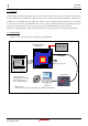
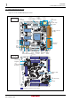
Overview 1 1.4 External View 1.4 External View Figure1.4.1 shows the external view of M3A-HS60. Figure1.4.1 External View of M3A-HS60 Rev.1.
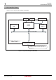
Overview 1 1.5 M3A-HS60 Block Diagram 1.5 M3A-HS60 Block Diagram Figure1.5.1 shows the system block diagram of M3A-HS60. H-UDI Serial port connector SH7206 200MHz Flash memory 4MB 16 or 32 16 User I/O Connector SDRAM 16MB x 2 16 or 32 External:66.67MHz SH7206 CPU Board M3A-HS60 Extension connector Enables to connect extension boards, or enables to monitor all of bus and peripheral I/O signals. Figure1.5.1 System Block Diagram of M3A-HS60 Rev.1.
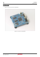
Overview 1 1.6 M3A-HS60 Board Overview 1.6 M3A-HS60 Board Overview Figure1.6.1 shows the M3A-HS60 board overview.
Overview 1 1.6 M3A-HS60 Board Overview Table1.6.1 lists main components mounted in M3A-HS60. Table1.6.1 Main Components Mounted in M3A-HS60 Recommended parts’ Symbol Component name Note number for not mounted components (Makers) U1 CPU SH7206 (by Renesas) U2 Clock Buffer Not mounted U3 Flash Memory M5M29KT331AVP CY2305SC-1 (by Cypress) (by Renesas) U4,U7 Address Shift Buffer U5,U8 SDRAM U6 Logic IC U9 RS-232C Driver U10 3.3V Power Regulator U11 Reset IC U12 1.
Overview 1 1.7 M3A-HS60 Memory Mapping 1.7 M3A-HS60 Memory Mapping Figure1.7.1 shows the memory mapping example of SH7206 in the M3A-HS60.
Overview 1 1.8 Absolute Maximum Ratings 1.8 Absolute Maximum Ratings Table1.8.1 lists the absolute maximum ratings of M3A-HS60. Table1.8.1 Absolute Maximum Ratings of M3A-HS60 Symbol Parameter Rated Value Remarks VCC 5V System Power Supply Voltage -0.3V to 6.0V Relative to VSS 3VCC 3.3V System Power Supply Voltage -0.3V to 4.6V Relative to VSS 1.2VCC 1.25V System Power Supply Voltage -0.3V to 1.7V Relative to VSS Operating Ambient Temperature -5°C to 55°C No dewdrops allowed.
Overview 1 1.8 Absolute Maximum Ratings This is a blank page Rev.1.
Chapter2Functional Overview Chapter2 Functional Overview 2-1
Functional Overview 2 2.1 Functional Overview 2.1 Functional Overview Table2.1.1 lists the functional modules of M3A-HS60. Table2.1.1 Functional Modules of M3A-HS60 Sections 2.2 Function CPU Content SH7206 zInput(XIN)clock : 16.67MHz zBus clock : 66.67MHz,max zCPU clock : 200MHz,max 2.3 Memory Following items of memory are included z SDRAM: 32 Mbytes, max By switching a DIP switch, the following memories can be selected.
Functional Overview 2 2.2 CPU 2.2 CPU 2.2.1 SH7206 The M3A-HS60 contains SH7206, the 32-bit RISC microcomputer, which operates with a maximum 200MHz of CPU clock frequency. The SH7206 includes 128-Kbyte RAM, 8-Kbyte instruction cache and 8-Kbyte data cache, and it can deal with a wide range of applications from data processing to equipment control. The M3A-HS60 can be operated with a maximum 200MHz of CPU clock frequency (external bus 66.67MHz, max.) using a 16.67MHz input clock. Figure2.2.
Functional Overview 2 2.3 Memory 2.3 Memory The M3A-HS60 includes the internal RAM of the SH7206 (128 Kbytes), external Flash memory, and external SDRAM. These memory chips are detailed below. 2.3.1 SH7206's Internal RAM The SH7206 contains an internal 128-Kbyte RAM. 2.3.2 Flash Memory M5M29KT331AVP (included as standard equipment) The M3A-HS60 includes the Flash memory shown in Table2.3.1 as standard equipment. The memory can be used as the storage in which to save the user program.
Functional Overview 2 2.3.2 Flash Memory M5M29KT331AVP (included as standard equipment) Table2.3.
Functional Overview 2 2.3.3 External SDRAM 2.3.3 External SDRAM The M3A-HS60 includes two pcs. of 16-Mbyte SDRAM (for an external SDRAM) as standard equipment. The SH7206's internal bus state controller can be used to control the SDRAM. Note that the SDRAM can be switched between 32-bit bus access and 16-bit bus access. (For 16-bit bus access, only one pc. of 16-Mbyte SDRAM can be used.) Table2.3.3 lists SDRAM specifications used in M3A-HS60. Figure2.3.3 shows a block diagram of SDRAM. Table2.3.
Functional Overview 2 2.3.3 External SDRAM Table2.3.4 lists bus state controller settings for operation with the SH7206 Bus clock at 66.67MHz. Table2.3.4 Examples for Bus State Controller Settings (SDRAM Read/ Write) User Area CS3 Rev.1.
Functional Overview 2 2.3.
Functional Overview 2 2.4 Serial Port Interface 2.4 Serial Port Interface The SH7206 included in the M3A-HS60 contains a UART module. As for the M3A-HS60, SCIF channel 0 is connected to serial port connector. Figure2.4.1 shows a block diagram of serial port interface in the M3A-HS60. SH7206 RXD0 TXD0 RS-232C driver Serial port connector NC 1 2 3 4 GND 5 6 DCD# RxD TxD DTR# GND DSR# 7 RTS# 8 CTS# NC 9 RI# Figure2.4.1 Block Diagram of Serial Port Interface Rev.1.
Functional Overview 2 2.5 I/O Ports 2.5 I/O Ports As for the M3A-HS60, the SH7206's I/O ports are connected to the extension bus connector of the M3A-HS60 board. Some I/O ports are connected to DIP switches and LEDs of the M3A-HS60 board. Users are free to use these ports. Figure2.5.1 shows a block diagram of SH7206 I/O ports. Table2.5.1 shows the functions of SH7206 I/O ports. 3.
Functional Overview 2 2.5 I/O Ports Table2.5.1 Functions of SH7206 I/O Ports SH7206 Port Name Connection in the M3A-HS60 PA0-PA1 Serial port connector. PA2 Extension connector, SDRAM_SZ signal input. PA3,PA6,PA11,PA17, Extension connector. PA20,PA21 PA4-PA5 Flash memory and extension connector. PA7-PA9,PA13,PA22,PA23 SDRAM and extension connector. PA12 Flash memory, SDRAM and extension connector. PA13 SDRAM and extension connector. PA18 SW1-1 and extension connector.
Functional Overview 2 2.6 Power Supply Circuit 2.6 Power Supply Circuit The M3A-HS60 accepts a 5V power supply as its input, and generates 3.3V and 1.25V by using a regulator. The regulator used here is an output voltage variable type, so that any desired voltage can be generated by changing the resistance value. Figure2.6.1 shows a block diagram of power supply circuit in the M3A-HS60. Extension connector Extension connector SW1 SDRAM 5V Flash memory 5V -> 3.
Functional Overview 2 2.7 Clock Module 2.7 Clock Module The clock module in the M3A-HS60 consists of the following two blocks: • Output from a oscillator connected to EXTAL of the SH7206 • Ceramic resonator connected to EXTAL and XTAL The M3A-HS60 has a 16.67MHz oscillator connected. Furthermore, the bus clock output from the SH7206 is connected to the SDRAM via a damping resistor.
Functional Overview 2 2.8 Reset Module 2.8 Reset Module This module controls the reset signals connected to both the SH7206 and Flash memory mounted in the M3A-HS60. Figure2.8.1 shows a block diagram of the reset module in M3A-HS60. H-UDI connector RES# ResetIC output delay time,td=0.34 x Cd(pF)µsec = 34ms ResetIC output detection voltage,Vs = 1.25 x Flash memory = 2.5V ) Ra+Rb Rb ) RP# Extension connector Ra 10KW Reset IC M51957BFP Input Rb 10KW RESET# 3.3V 3.
Functional Overview 2 2.10 E10A-USB 2.10 E10A-USB Interface As for the M3A-HS60, a 36-pin H-UDI connector to connect it with the E10A-USB is mounted. Figure2.10.1 shows a block diagram of the E10A-USB interface. 3.3V 3.3V H-UDI connector (36-pin type) 2 4 6 8 10 12 14 16 18 20 22 24 26 28 30 GND GND GND GND GND GND GND GND GND SH7206 AUDCK AUDATA0 AUDATA1 AUDATA2 AUDATA3 AUDSYNC# N.C. N.C. TCK TMS GND TRST# (GND) GND TDI TDO GND GND ASEBRKAK#/ASEBRK# UVCC GND 32 RES# GND 34 GND GND 36 GND N.C.
Functional Overview 2 2.10 E10A-USB This is a blank page Rev.1.
Chapter3 Operational Specifications Chapter3 Operational Specifications 3-1
Operational Specifications 3 3.1 M3A-HS60 Connectors Outline 3.1 M3A-HS60 Connectors Outline Figure3.1.1 shows the M3A-HS60 connectors assignments. J4 J1 J7, J8 J2 J3, J5 J12 J13 J6 J11 J9 J10 Figure3.1.1 M3A-HS60 Connector Assignment Rev.1.
Operational Specifications 3 3.1.1 H-UDI Connector (J1) 3.1.1 H-UDI Connector (J1) The M3A-HS60 includes an H-UDI (J1) connector for connection to the E10A-USB emulator. Figure3.1.2 shows a pin arrangement of the H-UDI connector. 35 36 1 2 Board edge Top view of the Component side J1 Board edge Side view Figure3.1.2 Pin Arrangements of the H-UDI Connector Table3.1.1 lists pin assignments of H-UDI connector. Table3.1.
Operational Specifications 3 3.1.2 Serial Port Connector (J2) 3.1.2 Serial Port Connector (J2) The M3A-HS60 includes a serial port connector for serial communication (J2). Figure3.1.3 shows a pin assignment of serial port connector. 5 9 1 6 Board edge Top view of the Component side J2 5 9 1 6 Board edge Side view Figure3.1.3 Pin Arrangement of Serial Port Connector (J2) Table3.1.2 lists pin assignments of serial port connector. Table3.1.
Operational Specifications 3 3.1.3 External Power Supply Connectors(J3 and J5) 3.1.3 External Power Supply Connectors(J3 and J5) The M3A-HS60 has the through-hole for two external power supply connectors (J3 for 3.3 V and J5 for 1.25 V) for the SH7206. Figure3.1.4 shows a pin assignment of external power supply connectors. J3 J5 1 2 1 2 Top view of the Component side Board edge Figure3.1.4 Pin Arrangement of External Power Supply Connectors (J3 and J5) Table3.1.3, and Table3.1.
Operational Specifications 3 3.1.4 Power Supply Connector (J4) 3.1.4 Power Supply Connector (J4) The M3A-HS60 includes a power supply connector for the board itself. Figure3.1.5 shows a pin assignment of power supply connector. 1 2 Top view of the Component side Board edge J4 1 2 Board edge Side view Figure3.1.5 Pin Arrangement of Power Supply Connector (J4) Table3.1.5 lists pin assignments of power supply connector for the M3A-HS60. Table3.1.
Operational Specifications 3 3.1.5 User I/O Connectors (J6-J8) 3.1.5 User I/O Connectors (J6-J8) The through-hole for the extension connector pin connecting the pins of the on-chip peripheral functions (such as MTU2 and AD), which is suitable for the motor control of SH7206, is mounted on M3A-HS60. Figure3.1.6 shows a pin arrangement of extension connector. Note: The J6 connects the pins multiplexed to data bus (D31-D16) of SH7206. Therefore, the data bus D31–D16 becomes unusable when the J6 is used.
Operational Specifications 3 3.1.5 User I/O Connectors (J6-J8) Table3.1.7 Pin Assignments of Extension Connectors (J7 and J8) J7 Pin Signal Name J8 Pin Signal Name 1 D16/IRQ0/POE4#/AUDATA0/PD16 1 AN5/PF5 2 D17/IRQ1/POE5#/AUDATA1/PD17 2 AN6/DA0/PF6 3 D18/IRQ2/POE6#/AUDATA2/PD18 3 AN7/DA1/PF7 Rev.1.
Operational Specifications 3 3.1.5 User I/O Connectors (J6-J8) 3.1.6 Extension Connectors (J9-J13) The M3A-HS60 has the trough-hole for extension bus connectors to which the I/O pins of the SH7206 are connected. MIL Standard connectors can be mounted to J9–J13, and it is available for the connection to extension boards, or monitoring the SH7206 bus signals. The bus signals of SH7206 are connected with J10 (J12) of the terminal connector via J9 (J13).
Operational Specifications 3 3.1.5 User I/O Connectors (J6-J8) Table 3.1.8 to 3.1.12 list pin assignments of extension connector. Table3.1.8 Pin Assignment of Extension connector(J9) Pin Signal name Pin Signal name 1 NC 2 NC 3 EXCLK 4 A9 5 A8 6 A7 A6 8 A5 A4 10 A3 A1/PC1 7 9 11 A2 12 13 A0/PC0 14 CS0# 15 CS1#/POE5/PA11 16 CS2#/TCLKA/PA6 17 RASU#/PINT4/CS4#/PA20 18 CASU#/PINT5/CS5#/CE1A#/TIC5U/PA21 19 RESET# 20 GND Table3.1.
Operational Specifications 3 3.1.5 User I/O Connectors (J6-J8) Table3.1.10 Pin Assignments of Extension Connector(J13) Pin Signal Name Pin Signal Name 1 NC 2 NC 3 RD# 4 D15/TIOC4DS/PD15 5 D14/TIOC4CS/PD14 6 D13/TIOC4BS/PD13 D12/TIOC4AS/PD12 8 D11/TIOC3DS/PD11 D10/TIOC3CS/PD10 10 D9/TIOC3BS/PD9 D7 7 9 11 D8/TIOC3AS/PD8 12 13 D6 14 D5 15 D4 16 D3 17 D2 18 D1 19 D0 20 GND Table3.1.
Operational Specifications 3 3.1.5 User I/O Connectors (J6-J8) Table3.1.
Operational Specifications 3 3.2 Outline of Switches and LEDs 3.2 Outline of Switches and LEDs The M3A-HS60 includes switches and LEDs as its operational components. Figure3.2.1 shows the M3A-HS60 Operational Component Assignment. JP1 JP2 SW1 LED LED1 6-8 SW4 LED 2-5 SW2 SW3 SW5 SW6 Figure3.2.1 M3A-HS60 Operational Component Assignment Rev.1.
Operational Specifications 3 3.2.1 Power Supply Select Jumpers (JP1 and JP2) 3.2.1 Power Supply Select Jumpers (JP1 and JP2) The SH7206 uses 3.3V and 1.25V power supply voltages. The JP1 and JP2 allow the sources for the SH7206 power supply voltages (3.3V and 1.25V) to be selected. Figure3.2.2 shows the SH7206 Power Supply Voltage Select Jumpers Assignment (JP1 and JP2). Table3.2.1 and Table3.2.2 list jumper settings for selecting SH7206 power supply voltage.
Operational Specifications 3 3.2.2 Switch and LED Functions 3.2.2 Switch and LED Functions The M3A-HS60 includes six switches and eight LEDs. Figure3.2.3 shows the M3A-HS60 Switch and LED Pin Assignment. Table3.2.3 lists the switches mounted on M3A-HS60. ON OFF Top view of the component side SW1 LED6 PE14 LED7 PE15 LED8 LED2 PE2 LED3 PE8 LED4 PE10 LED5 SW2 3 2 1 ON PA18 PA19 PA24 PA25 PE1 SW4 4 PE11 5 LED1 SW5 ON SW3 1 RST NMI 2 3 SW6 4 1 2 3 4 MRES Figure3.2.
Operational Specifications 3 3.2.2 Switch and LED Functions Table3.2.4 lists the functions of the switch SW4. : Initial Setting Table3.2.4 Functions of the Switch SW4 No.
Operational Specifications 3 3.3 Outline Dimensions of M3A-HS60 3.3 Outline Dimensions of M3A-HS60 Figure3.3.1 shows the outline dimensions of M3A-HS60. Connectors can be mounted on J6-J13 so that it is easy to connect extension boards. Unit :mm Figure3.3.1 Outline Dimensions of M3A-HS60 Rev.1.
Operational Specifications 3 3.3 Outline Dimensions of M3A-HS60 This is a blank page Rev.1.
Appendix M3A-HS60 Schematics A-1
This is a blank page A-2
1 2 3 4 5 SH-2A SH7206 CPU BOARD M3A-HS60 SCHEMATICS A A B TITLE PAGE INDEX CPU SH7206 FLASH SDRAM UDI/RESET/UART/POWER BUS CONNECTORS/PUSH SW OTHERS 1 2 3 4 5 6 7 B Note: VCC = 5V 3VCC = 3.3V 1.2VCC = 1.25V C R RA C CE CP [Note] D = = = = = C Fixed Resistors Resistor Array Ceramic Caps Tantalum Electrolytic Caps Decoupling Caps :not mounted D CHANGE RENESAS SOLUTIONS CORPORATION DRAWN SCALE DATE Ver. 1.
1 2 3 4 5 3VCC_CPU 3AVCC 3VCCQ 1.
1 2 3 4 5 [2,4,6] D[0:31] FVDD 3VCC R17 0Ω 1 R21 4.7KΩ R19 4.7KΩ 3VCC B R22 4.7KΩ [2,5,6] _RESET [2,6] _CS0 [2,6] _RD [2,4,6] _WE0/_DQMLL [5] FVDD U3 15 13 10 9 16 17 48 1 2 3 4 5 6 7 8 18 19 20 21 22 23 24 25 RY/BY NC A20 A19 A18 A17 A16 A15 A14 A13 A12 A11 A10 A9 A8 A7 A6 A5 A4 A3 A2 A1 A0 47 12 BYTE RP 26 28 11 CE OE WE 14 FLASH_WP# C A DQ15/A-1 DQ14 DQ13 DQ12 DQ11 DQ10 DQ9 DQ8 DQ7 DQ6 DQ5 DQ4 DQ3 DQ2 DQ1 DQ0 M5M29KT331AVP R20 4.
1 [2,3,6] 2 3 4 5 D[0:31] A A SVDD0 H5 SVDD0 [2,3,6] A[0:25] A[0:25] 3VCC R23 SA[1:15] SVDDQ0 1 1 0Ω H6 SVDDQ0 R26 0Ω 3VCC DUMPING REGISTER for SDRAM R27 0Ω [2,6] B R24 4.
1 2 3 4 5 H-UDI INTERFACE 3VCC 3VCC 3VCC SERIAL CONNECTOR(COM) RA10 A4.7KΩ R39 4.7KΩ 1 C1 0.1µF C1C2+ C3 0.
1 2 3 Extension Connector 4 Extension Bus Connector 5 3VCC R64 R65 0Ω 0Ω VCC J6 A AN3 [2,4] TIOC4AS [2,4] TIOC4BS [2,4] TIOC4CS [2] TIOC3B/PE9 [2] TIOC4A/PE12 [2] _MRES/TIOC4B [2] TIOC3D/PE11 [2] TIOC4D/PE15 [2] TIOC4C/PE14 [2,4] IRQ4/PD20 [2,4] IRQ5/PD21 [2,4] IRQ6/PD22 [2,4] IRQ3/PD19 [2] AN2 [2] AN3 [2] AN4 [2,4] [2,4] [2,4] [2,4] [2] [2] R66 0Ω TIOC4B _MRES TIOC3D/PE11 TIOC4D/PE15 TIOC4C/PE14 IRQ4/PD20 IRQ5/PD21 IRQ6/PD22 IRQ3/PD19 AN2 AN3 AN4 R67 0Ω PD28 PD29 PD30 PD31 PD28 PD29 PD30 P
1 2 3 4 5 TEST PIN A A VCC H9 H10 3VCC H11 1.2VCC MH1 H12 1 1 1 1 VCC 3VCC 1.2VCC GND 1 1 MOUNT-HOLE H13 MH2 1 GND 1 B 1 B UNUSED LOGIC MOUNT-HOLE MH3 13 1 12 MOUNT-HOLE U6F HD74LVC14T MH4 C C AGND-GND 1 R81 1 0Ω 1 MOUNT-HOLE D D CHANGE RENESAS SOLUTIONS CORPORATION DRAWN SCALE DATE Ver. 1.
This is a blank page
SH7206 CPU Board M3A-HS60 User's Manual Publication Data June 1,2005 Rev. 1.00 Published by Renesas Technology Corp. Renesas Solutions Corp. © 2005. Renesas Technology Corp., All rights reserved. Printed in Japan.
M3A-HS60 User's Manual