REJ10J0952-0100 SH7125 CPU Board M3A-HS25 32 User's Manual Renesas 32-Bit RISC Microcomputers SuperH RISC engine Family / SH7125 Group TM Rev. 1.
Microsoft, MS-DOS, Windows and Windows.NET are registered trademarks of Microsoft Corporation of the U.S. in the U.S. and other countries. IBM and AT are registered trademarks of International Business Machines Corporation of the U.S. Adobe and Acrobat are registered trademarks of Adobe Systems Incorporated. All other brand names and product names are registered trademarks or trademarks of the respective proprietors.
Revision History Rev. SH7125 CPU Board M3A-HS25User's Manual Date of Issue Content of Revision Page 1.0 July 21, 2006 - Page First edition issued.
Table of Contents Chapter1 Overview .............................................................................................................................. 1-1 1.1 Overview .................................................................................................................................................................... 1-2 1.2 Configuration .................................................................................................................................................
Chapter1Overview Chapter1 Overview 1-1
Overview 1 1.1 Overview 1.1 Overview The M3A-HS25 is the CPU board designed for users to evaluate the functionality and performance of the SH7125 group of Renesas Technology original microcomputers, as well as develop and evaluate the application software for this group of microcomputers.
Overview 1 1.3 External Specifications 1.3 External Specifications Table1.3.1 lists external specifications of M3A-HS25. Table1.3.1 External Specifications of M3A-HS25 No. Item Content SH7125 1 CPU • Input(XIN) clock : 12.5MHz • CPU clock : 50MHz, max • Peripheral clock : 25MHz, max • On-chip memory Flash memory : 128KB RAM : 8KB 2 Connectors 3 LED 4 Switches 5 User through-hole 6 External dimensions Rev.1.
Overview 1 1.4 External View 1.4 External View Figure1.4.1 shows the external view of M3A-HS25. Figure1.4.1 External View of M3A-HS25 Rev.1.
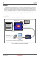
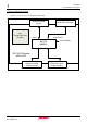
Overview 1 1.5 M3A-HS25 Block Diagram 1.5 M3A-HS25 Block Diagram Figure1.5.1 shows the system block diagram of M3A-HS25. H-UDI connector (14-pin) User Trough-hole area (12×8pc.) Serial Port Connector SCI0 or SCI1 H-UDI XIN(12.5MHz) SH7125 (50MHz) SH7125 CPU board M3A-HS25 Extension Connector (Common use for 48 pins version) Extension Connector (Exclusive use for 64 pins version) Figure1.5.1 System Block Diagram of M3A-HS25 Rev.1.
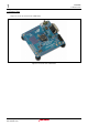
Overview 1 1.6 M3A-HS25 Board Overview 1.6 M3A-HS25 Board Overview Figure1.6.1 shows the M3A-HS25 board overview.
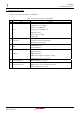
Overview 1 1.6 M3A-HS25 Board Overview Table1.6.1 lists main components mounted in M3A-HS25. Table1.6.1 Main Components Mounted in M3A-HS25 Parts number for Symbol Parts Name Remarks recommended components that are not mounted U1 CPU SH7125 (Renesas) U1 CPU Socket NQPACK064SD U2 RS-232C Driver U3 Reset IC U4 Logic IC U5 Logic IC X1 Oscillator 12.
Overview 1 1.7 M3A-HS25 Memory Mapping 1.7 M3A-HS25 Memory Mapping Figure1.7.1 show a memory mapping example of SH7125 in the M3A-HS25.
Overview 1 1.8 Absolute Maximum Ratings 1.8 Absolute Maximum Ratings Table1.8.1 lists the absolute maximum ratings of M3A-HS25. Table1.8.1 Absolute Maximum Ratings of M3A-HS25 Symbol Parameter Rated Value Remarks VCC 5V System Power Supply Voltage -0.3V to 6.0V Relative to VSS Topr Operating Ambient Temperature -5°C to 55°C No dewdrops allowed. Use in corrosive gas environment prohibited. Tstr Storage Ambient Temperature -10°C to 60°C No dewdrops allowed.
Overview 1 1.8 Absolute Maximum Ratings * This is a blank page * Rev.1.
Chapter2Functional Overview Chapter2 Functional Overview 2-1
Functional Overview 2 2.1 Functional Overview 2.1 Functional Overview The M3A-HS25 is the SH7125 CPU board that has functions listed in Table2.1.1. Table2.1.1 lists functional modules of M3A-HS25. Table2.1.1 Functional Modules of M3A-HS25 Section 2.2 Function CPU Content SH7125 • Input(XIN) clock : 12.5MHz • CPU clock : 50MHz, max • On-chip Memory - Flash memory : 128KB - RAM : 8KB 2.3 Serial Port Interface Connects SCI0 or SCI1 of the SH7125 to the UART connector 2.
Functional Overview 2 2.2 CPU 2.2 CPU The M3A-HS25 contains the 32-bit RISC microcomputer SH7125 that operates with a maximum 50MHz of CPU clock frequency. The SH7125 includes 128-Kbyte flash memory, and 8-Kbyte SRAM, making it useful in a wide range of applications from data processing to equipment control. The M3A-HS25 can be operated with a maximum 50MHz of CPU clock frequency using a 12.5MHz input clock. Figure2.2.1 shows the block diagram of SH7125 in the M3A-HS25.
Functional Overview 2 2.3 Serial Port Interface 2.3 Serial Port Interface The SH7125 included in the M3A-HS25 contains a UART module. In the M3A-HS25, the pins of SCI channel 0 or SCI channel 1 can be connected to J2 (Serial Port connector). The pins of SCI channel 1 (RXD1(PA3) pin and TXD 1 (PA4)pin) are also connected to H-UDI connector, and extension connector (J5, J7). Switch the setting of the JP3 and JP4 according to the connector used. Figure2.3.
Functional Overview 2 2.4 I/O Ports 2.4 I/O Ports In the M3A-HS25, all of the SH7125's I/O ports are connected to the extension connector. Some I/O ports are connected to DIP switches and LEDs of the M3A-HS25 board. Users are free to use these ports. Figure2.4.1 shows the block diagram of DIP switch and LEDs in the M3A-H25. Table2.4.1 shows functions of SH7125 I/O ports in the M3A-HS25.
Functional Overview 2 2.4 I/O Ports Table2.4.
Functional Overview 2 2.5 Clock Module 2.5 Clock Module The clock module in the M3A-HS25 consists of the following two blocks: • • Output from a oscillator connected to EXTAL of the SH7125 Ceramic resonator connected to EXTAL and XTAL The M3A-HS25 has a 12.5MHz oscillator connected to it as standard specification. Figure2.5.1 shows the block diagram of clock module. Oscillator CLK SH7125 * R21 EXTAL XTAL Ceramic Resonators 12.5MHz *:To mount the ceramic oscillator, remove R21.
Functional Overview 2 2.6 Reset Module 2.6 Reset Module This module controls the reset signal connected to the SH7125 mounted on the M3A-HS25. Figure2.6.1 shows the block diagram of reset module in the M3A-HS25. Reset IC output delay time:td = 0.34 × Cd(pF)usec = 34ms Reset IC output detection voltage:Vs = 1.25 × (Ra+Rb)/Rb = 3.
Functional Overview 2 2.7 Interrupt Switches 2.7 Interrupt Switches In the M3A-HS25, the switch is connected with the IRQ0 pin and NMI pin of the SH7125. Figure2.7.1 shows the interrupt block diagram in the M3A-HS25. VCC SH7125 NMI SW5 NMI switch VCC PA2/IRQ0/SCK0 SW6 IRQ0 switch Figure2.7.1 Interrupt Block Diagram Rev.1.
Functional Overview 2 2.8 E10A-USB Interface 2.8 E10A-USB Interface The M3A-HS25 has a 14-pin H-UDI connector included in it for connection to the E10A-USB. TMS pins and TRST pins of SH7125 are multiplexed with transmit/receive pins of SCI channel 1. When H-UDI connector is used, make sure that the settings of JP3 and JP4 are set to 1-2 side.
Chapter3Operational Specifications Chapter3 Operational Specifications 3-1
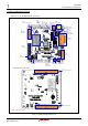
Operational Specifications 3 3.1 M3A-HS25 Connectors Outline 3.1 M3A-HS25 Connectors Outline Figure3.1.1 shows the M3A-HS25 connector assignments. J3 Power Supply connector J4 External Power Supply Connector (Not mounted) J7 Extension connector (Not mounted) J2 Serial Port Connector J1 H-UDI Connector < Top view of the solder side > J5 Extension Connector (Not mounted) J6 Extension Connector (Not mounted) Figure3.1.1 M3A-HS25 Connector Assignments Rev.1.
Operational Specifications 3 3.1.1 H-UDI Connector (J1) 3.1.1 H-UDI Connector (J1) M3A-HS25 has the 14-pin H-UDI (J1) connector included in it for connection to the E10A-USB emulator. Figure3.1.2 shows a pin assignment of H-UDI (J1) connector. 7 6 5 4 3 2 1 14 13 12 11 10 9 8 Board edge Top view of the component side J1 Side view Board edge Figure3.1.2 Pin Assignment of H-UDI (J1) Connector Table 3.1.1 lists pin assignments of H-UDI connector (J1). Table 3.1.
Operational Specifications 3 3.1.2 Serial Port Connector (J2) 3.1.2 Serial Port Connector (J2) The M3A-HS25 includes a serial port connector (J2) for serial communication. Figure 3.1.3 shows a pin assignment of serial port connector. 1 5 6 9 Top view of the component side Board edge Board edge 1 5 6 9 Side view Figure 3.1.3 Pin Assignment of Serial Port Connector (J2) Table 3.1.2 lists pin assignments of serial port connector. Table 3.1.
Operational Specifications 3 3.1.3 Power Supply Connector (J3) 3.1.3 Power Supply Connector (J3) The M3A-HS25 includes a power supply connector for the board itself. Figure 3.1.4 shows a pin assignment of power supply connector. 1 2 1 2 Top view of the component side Board edge Side view Board edge Figure 3.1.4 Pin Assignment of Power Supply Connector (J3) Table 3.1.3 lists a pin assignment of power supply connector for the M3A-HS25. Table 3.1.
Operational Specifications 3 3.1.4 External Power Supply Connectors (J4) 3.1.4 External Power Supply Connectors (J4) The M3A-HS25 includes external power supply connectors for the SH7125. Figure3.1.5 shows a pin assignment of power supply connector. 1 2 Top view of the component side J4 VCC Board edge Figure3.1.5 Pin Assignment of Power Supply Connector (J4) Table 3.1.4 lists pin assignments of power supply connector for the SH7125. Table 3.1.
Operational Specifications 3 3.1.5 Extension Connectors (J5,J6) 3.1.5 Extension Connectors (J5,J6) The M3A-HS25 includes extension connectors to which the I/O pins of the SH7125 are connected. MIL Standard connectors can be connected to J5 and J6, allowing the user to create an extension board or to monitor the I/O, etc. In addition, pins of SH7124 (48-pin version) is arranged in the extension connector (J5), so it is possible to be used for a brief evaluation. Figure 3.1.
Operational Specifications 3 3.1.5 Extension Connectors (J5,J6) Table 3.1.5 shows pin assignments of extension connector (J5). Table 3.1.
Operational Specifications 3 3.1.5 Extension Connectors (J5,J6) Table 3.1.6 lists pin assignments of Extension Connector (J6). Table 3.1.
Operational Specifications 3 3.1.6 Extension Connector (J7) 3.1.6 Extension Connector (J7) Extension connector(J7) connects the pins necessary for writing a on-chip flash memory of SH7125. Figure 3.1.7 shows pin assignments of the extension connectors. Board edge 13 11 J7 9 7 3 1 5 4 2 6 8 10 12 14 Top view of the component side Board edge Figure 3.1.7 Pin assignments of the Extension Connector (J7) Table 3.1.7 lists pin assignments of the extension connector(J7). Table 3.1.
Operational Specifications 3 3.2 User Through-hole 3.2 User Through-hole M3A-HS25 has the user trough-holes (12 x 8pc.) The user trough-holes are not connected to VCC, GND and signal lines, so users are free to use them. Figure 3.2.1 shows pin assignments of the user trough-hole. Board edge Top view of the component side 1 2 3 4 5 6 7 8 A B C D E F G H J K L M UH1 Board edge Figure 3.2.1 Pin assignments of the user trough-hole Rev.1.
Operational Specifications 3 3.3 Outline of Operational Components 3.3 Outline of Operational Components The M3A-HS25 includes switches, jumpers and LEDs as its operational components. Figure 3.3.1 shows the M3A-H25 operational component assignment.
Operational Specifications 3 3.3.1 SH7125 Power Supply Select Jumper (JP1) 3.3.1 SH7125 Power Supply Select Jumper (JP1) The JP1 allows the sources for the SH7125 power supply voltages to be selected. Figure 3.3.2 shows the SH7125 power supply voltage select jumper (JP1) assignment. Table 3.3.1 lists jumper setting for selecting SH7125 power supply voltage (JP1). Top view of the component side 3 1 JP1 PWRSEL Board edge Board edge Figure 3.3.
Operational Specifications 3 3.3.2 FWE Pin Select Jumper (JP2) 3.3.2 FWE Pin Select Jumper (JP2) ________________ _____________________ The JP2 allows the connection for the FWE/ASEBRK/ASEBRKAK pin to be selected. Figure 3.3.3 shows the FWE pin select jumper (JP2) assignment. Table 3.3.2 lists the jumper setting for selecting FWE pin (JP2). Top view of the component side 3 1 JP2 FWESEL Board edge Board edge Figure 3.3.3 FWE Pin Select Jumper (JP2) Assignment Table 3.3.
Operational Specifications 3 3.3.3 Serial Port Select Jumpers (JP3,JP4) 3.3.3 Serial Port Select Jumpers (JP3,JP4) By setting the JP3 and JP4, the serial port of SH7125 connected to the serial port connector (J2) can be selected. Figure 3.3.4 shows the Serial port select jumper assignment. Table 3.3.3 and Table 3.3.4 list the jumper setting for selecting Serial port (JP3, JP4). Top view of the component side 3 JP4 RxD SEL 1 3 1 JP3 TxD SEL Board edge Board edge Figure 3.3.
Operational Specifications 3 3.3.4 Switch and LED Functions 3.3.4 Switch and LED Functions The M3A-HS25 includes six switches and seven LEDs. Table 3.3.5 lists switches mounted on M3A-HS25. Table 3.3.5Switches Mounted on M3A-HS25 No. Function Remarks SW1 System power on/off switch - SW2 System reset input switch ref. section 2.6 SW3 DIP switch for users PB1, PB2, PB3 and PB5 are pulled up.
Operational Specifications 3 3.3.4 Switch and LED Functions Table 3.3.8 lists functions of LEDs mounted in M3A-HS25. Table 3.3.8 Functions of LEDs Mounted in M3A-HS25 No.
Operational Specifications 3 3.4 Package Dimensions of M3A-HS25 3.4 Package Dimensions of M3A-HS25 Figure 3.4.1 shows package dimensions of M3A-HS25. Figure 3.4.1 Package Dimensions of M3A-HS25 Rev.1.
Appendix M3A-HS25 SCHEMATICS A-1
* This is a blank page * A-2
1 2 3 4 5 SH7125 CPU BOARD M3A-HS25 SCHEMATICS A A TITLE PAGE INDEX CPU SH7125 UDI/RESET/UART/POWER CONNECTORS/PUSH SW OTHERS B 1 2 3 4 5 B Note: VCC = 5V C C R RA C CE CP [Note] = = = = = Fixed Resistors Resistor Array Ceramic Caps Tantalum Electrolytic Caps Decoupling Caps : not mounted D D CHANGE RENESAS SOLUTIONS CORPORATION DRAWN SCALE DATE Ver. 1.
1 2 3 4 5 VCC AVCC R1 0Ω 1 H1 AVCC A A PA0 PA1 PA2 PA5 PA6 PA10 PA11 PA12 PA13 PA14 PA15 38 36 34 30 29 25 23 21 20 19 18 PA0/POE0#/RXD0 PA1/POE1#/TXD0 PA2/IRQ0/SCK0 PA5/IRQ3/SCK1 PA6/TCLKA PA10/RXD0 PA11/TXD0/ADTRG# PA12/SCK0 PA13/SCK1 PA14/RXD1 PA15/TXD1 PB1/TIC5W PB2/IRQ0/POE0# PB3/IRQ1/POE1#/TIC5V PB5/IRQ3/TIC5U PB16/POE3# PB1 PB2 PB3 PB5 PB16 51 50 49 48 62 PB1/TIC5W PB2/IRQ0/POE0# PB3/IRQ1/POE1#/TIC5V PB5/IRQ3/TIC5U PB16/POE3# 52 AVSS [3,4] [3,4] [3,4] [3,4] [4] PA0/POE0#/RXD0 PA
1 2 3 4 5 H-UDI INTERFACE SERIAL CONNECTOR(COM) VCC R23 4.7KΩ R24 4.7KΩ R25 4.7KΩ R26 4.7KΩ R27 4.7KΩ VCC VCC R28 4.7KΩ 1 2 3 4 5 6 7 TRST#/RXD1/PA3 E10A_ASEBRK# TMS/TXD1/PA4 [2,4] PA4/IRQ2/TXD1/TMS [2,4] PA8/TCLKC/RXD2/TDI C1 0.1µF VCC UVCC NC TCK _TRST TDO _ASEBRAK TMS TDI _RES R29 4.7KΩ 8 C3 0.1µF GND GND GND GND GND 9 10 12 13 14 R30 4.7KΩ ASEMD0# [2] UART connector mount hole = GND 2 3 16 3 4 C1C2+ R1OUT T1IN R2OUT T2IN V- 6 SP3232E R1IN T1OUT R2IN T2OUT C2 0.
1 2 3 4 5 Extension Connector USER PROTOTYPE VCC NMI SWITCH CIRCUIT VCC UH1 R53 R52 10KΩ 0Ω U4C A R55 100Ω 5 NMI SWITCH 0Ω U4D 6 9 74LVC14 SW5 B3SN-3012 R54 8 R56 NMI 0Ω 74LVC14 + CE7 4.
1 2 3 4 5 TEST PIN A A MH1 VCC H9 H10 1 1 VCC GND H11 H12 1 1 1 1 MOUNT-HOLE MH2 VCC GND 1 B 1 B MOUNT-HOLE MH3 1 1 MOUNT-HOLE MH4 C C AGND-GND 1 R62 0Ω 1 MOUNT-HOLE D D CHANGE RENESAS SOLUTIONS CORPORATION DRAWN SCALE DATE Ver. 1.
This is a blank page
SH7125 CPU Board M3A-HS25 User's Manual Publication Data July 21, 2006 Rev. 1.0 Published by Renesas Technology Corp. Renesas Solutions Corp. © 2006. Renesas Technology Corp., All rights reserved. Printed in Japan.
M3A-HS25 User's Manual