
Datasheet


M32C/87 Group (M32C/87, M32C/87A, M32C/87B) 1. Overview
REJ03B0127-0151 Rev.1.51 Jul 31, 2008
Page 20 of 85
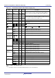
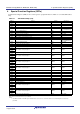
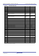
Table 1.16 Pin Functions (100-Pin and 144-Pin Packages) (2/4)
I: Input O: Output I/O: Input and output
NOTE:
1. The CAN pins cannot be used in M32C/87B. Only CAN0 pins can be used in M32C/87A.
Type Symbol
I/O
Type
Supply
Voltage
Description
Main clock
input
XIN I VCC1 Input/output pins for the main clock oscillation circuit. Connect a
ceramic resonator or crystal oscillator between XIN and XOUT. To
apply an external clock, apply it to XIN and leave XOUT open.
Main clock
output
XOUT O VCC1
Sub clock
input
XCIN I VCC1 Input/output pins for the sub clock oscillation circuit. Connect a
crystal oscillator between XCIN and XCOUT. To apply an external
clock, apply it to XCIN and leave XCOUT open.
Sub clock
output
XCOUT O VCC1
BCLK output BCLK O VCC2 Bus clock output pin.
Clock output CLKOUT O VCC2
The CLKOUT pin outputs the clock having the same frequency as
fC, f8, or f32.
INT interrupt
input
INT0 to INT2
I VCC1
INT
interrupt input pins.
INT3
to INT5
I VCC2
NMI
interrupt
input
NMI
I
VCC1 NMI interrupt input pin. Connect the NMI pin to VCC1 via a
resistor when the NMI interrupt is not used.
Timer A TA0OUT to
TA4OUT
I/O VCC1 Timer A0 to A4 input/output pins.
(TA0OUT is N-channel open drain output.)
TA0IN to
TA4IN
I VCC1 Timer A0 to A4 input pins.
Timer B TB0IN to
TB5IN
I VCC1 Timer B0 to B5 input pins.
Three-phase
motor control
timer output
U, U
, V, V,
W, W
O VCC1 Three-phase motor control timer output pins.
Serial
interface
CTS0
to CTS5
I VCC1 Input pins to control data transmission.
RTS0
to RTS5
O VCC1 Output pins to control data reception.
CLK0 to CLK5 I/O VCC1 Serial clock input/output pins.
RXD0 to RXD5 I VCC1 Serial data input pins.
TXD0 to TXD5 O VCC1 Serial data output pins.
(TXD2 is N-channel open drain output.)
I
2
C mode SDA0 to SDA4 I/O VCC1 Serial data input/output pins.
(SDA2 is N-channel open drain output.)
SCL0 to SCL4 I/O VCC1 Serial clock input/output pins.
(SCL2 is N-channel open drain output.)
Serial
interface
special function
STXD0 to
STXD4
O VCC1 Serial data output pins when slave mode is selected.
(STXD2 is N-channel open drain output.)
SRXD0 to
SRXD4
I VCC1 Serial data input pins when slave mode is selected.
SS0
to SS4
I VCC1 Control input pins used in the serial interface special mode.
IrDA
IrDAIN
I VCC1 IrDA serial data input pin.
IrDAOUT
O VCC1 IrDA serial data output pin.
CAN
(1)
CAN0IN,
CAN1IN
I VCC1 Received data input pins for the CAN communication function.
CAN0OUT,
CAN1OUT
O VCC1 Transmit data output pins for the CAN communication function.
CAN1WU
I VCC1 CAN wake-up interrupt input pin.