
Datasheet


M32C/87 Group (M32C/87, M32C/87A, M32C/87B) 1. Overview
REJ03B0127-0151 Rev.1.51 Jul 31, 2008
Page 19 of 85
1.5 Pin Functions
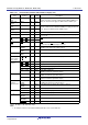
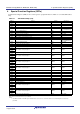
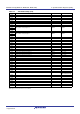
Table 1.15 Pin Functions (100-Pin and 144-Pin Packages)
(1/4)
I: Input O: Output I/O: Input and output
Type Symbol
I/O
Type
Supply
Voltage
Description
Power supply
VCC1,VCC2
VSS
−−Apply 3.0 to 5.5 V to pins VCC1 and VCC2, and 0 V to the VSS pin.
The input condition of VCC1 ≥ VCC2 must be met.
Analog power
supply input
AVCC
AVSS
− VCC1 Power supply input pins to the A/D converter and D/A converter.
Connect the AVCC pin to VCC1, and the AVSS pin to VSS.
Reset input RESET
I VCC1 The MCU is placed in the reset state while applying an “L” signal to
the RESET
pin.
CNVSS CNVSS I VCC1 This pin switches processor mode. Apply an “L” to the CNVSS pin
to start up in single-chip mode, or an “H” to start up in
microprocessor mode (mask ROM, flash memory version) and boot
mode (flash memory version).
External data
bus width
select input
BYTE I VCC1 This pin switches a data bus width in external memory space 3. A
data bus is 16 bits wide when the BYTE pin is held “L” and 8 bits
wide when it is held “H”. Fix to either “L” or “H”.
Apply an “L” to the BYTE pin in single-chip mode.
Bus control
Pins
D0 to D7 I/O VCC2 Data (D0 to D7) input/output pins while accessing an external
memory space with separate bus.
D8 to D15 I/O VCC2 Data (D8 to D15) input/output pins while accessing an external
memory space with 16-bit separate bus.
A0 to A22 O VCC2 Address bits (A0 to A22) output pins.
A23
O VCC2 Inverted address bit (A23) output pin.
A0/D0 to
A7/D7
I/O VCC2 Data (D0 to D7) input/output and 8 low-order address bits (A0 to
A7) output are performed by time-sharing these pins while
accessing an external memory space with multiplexed bus.
A8/D8 to
A15/D15
I/O VCC2 Data (D8 to D15) input/output and 8 middle-order address bits (A8
to A15) output are performed by time-sharing these pins while
accessing an external memory space with 16-bit multiplexed bus.
CS0
to CS3 O VCC2 Chip-select signal output pins used to specify external devices.
WRL
/WR
WRH/BHE
RD
O VCC2
WRL, WRH, (WR, BHE) and RD signal output pins. WRL and WRH
can be switched with WR
and BHE by a program.
•WRL, WRH and RD are selected:
If external data bus is 16 bits wide, data is written to an even
address in external memory space while an “L” is output from the
WRL
pin. Data is written to an odd address while an “L” is output
from the WRH
pin. Data is read while an “L” is output from the
RD
pin.
•WR
, BHE and RD are selected:
Data is written while an “L” is output from the WR
pin. Data is
read while an “L” is output from the RD
pin. Data in odd address
is accessed while an “L” is output from the BHE pin. Select WR,
BHE
and RD when an external data bus is 8 bits wide.
ALE O VCC2 ALE signal is used for the external devices to latch address signals
when the multiplexed bus is selected.
HOLD
I VCC2 The MCU is placed in a hold state while an “L” signal is applied to
the HOLD
pin.
HLDA
O VCC2 The HLDA pin outputs an “L” while the MCU is placed in a hold
state.
RDY
I VCC2 Bus is placed in a wait state while an “L” signal is applied to the
RDY
pin.