
Datasheet


Rev.2.10 Aug 25, 2006 page 66 of 67
REJ03B0061-0210
M16C/6N Group (M16C/6NL, M16C/6NN) 5. Electric Characteristics
Under development
This document is under development and its contents are subject to change.
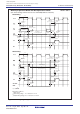
Figure 5.19 Timing Diagram (8)
Read timing
Write timing
Memory Expansion Mode and Microprocessor Mode
(For 3-wait setting, external area access and multiplexed bus selection)
BCLK
CSi
ALE
RD
ADi
/DBi
ADi
BHE
BCLK
CSi
ALE
ADi
/DBi
tcyc
td(BCLK-AD)
40ns.max
tcyc
Data output
th(BCLK-CS)
6ns.min
td(BCLK-CS)
40ns.max
td(BCLK-ALE)
40ns.max
th(BCLK-ALE)
-4ns.min
td(BCLK-RD)
40ns.max
th(BCLK-RD)
0ns.min
tSU(DB-RD)
50ns.min
th(RD-DB)
0ns.min
th(RD-AD)
(0.5 ✕ tcyc-10)ns.min
th(BCLK-AD)
4ns.min
td(BCLK-CS)
40ns.max
td(BCLK-AD)
40ns.max
th(BCLK-DB)
4ns.min
th(BCLK-WR)
0ns.min
th(WR-AD)
(0.5 ✕ tcyc-10)ns.min
th(BCLK-AD)
4ns.min
th(BCLK-CS)
4ns.min
td(BCLK-ALE)
40ns.max
td(BCLK-WR)
40ns.max
t
-4ns.min
th(WR-DB)
(0.5 ✕ tcyc-10)ns.min
Data input
Address
Address
ADi
BHE
WR, WRL
WRH
td(AD-ALE)
(0.5 ✕ tcyc-40)ns.min
td(AD-RD)
0ns.min
tdZ(RD-AD)
8ns.max
tac3(RD-DB)
td(BCLK-DB)
50ns.max
(0.5 ✕ tcyc-10)ns.min
th(WR-CS)
td(AD-WR)
0ns.min
th(RD-CS)
(0.5 ✕ tcyc-10)ns.min
td(AD-ALE)
(0.5 ✕ tcyc-40)ns.min
(2.5 ✕ tcyc-60)ns.max
(no multiplex)
(no multiplex)
tcyc =
1
f(BCLK)
Measuring conditions :
VCC = 3.3 V
Input timing voltage : V
IL = 0.6 V, VIH = 2.7 V
Output timing voltage : V
OL = 1.65 V, VOH = 1.65 V
td(DB-WR)
(2.5 ✕ tcyc-50)ns.min
h(BCLK-ALE)
(0.5 ✕ tcyc-15)ns.min
th(ALE-AD)
VCC = 3.3 V