
Datasheet


Rev.2.10 Aug 25, 2006 page 33 of 67
REJ03B0061-0210
M16C/6N Group (M16C/6NL, M16C/6NN) 5. Electric Characteristics
Under development
This document is under development and its contents are subject to change.
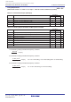
Table 5.3 Recommended Operating Conditions (2)
(1)
Main clock input oscillation No wait Mask ROM version VCC = 3.0 to 5.5 V
frequency
(2) (3) (4)
Flash memory version
Sub clock oscillation frequency
On-chip oscillation frequency
PLL clock oscillation frequency
CPU operation clock
VCC = 3.0 to 5.5 V
PLL frequency synthesizer stabilization wait time
32.768
1
MHz
kHz
MHz
MHz
MHz
ms
0
16
0
16
50
24
24
20
f(XIN)
f(XCIN)
f(Ring)
f(PLL)
f(BCLK)
t
su(PLL)
ParameterSymbol
Typ.Min.
Standard
Unit
Max.
NOTES:
1. Referenced to VCC = 3.0 to 5.5 V at Topr = –40 to 85°C unless
otherwise specified.
2. Relationship between main clock oscillation frequency and supply
voltage is shown right.
3. Execute program/erase of flash memory by VCC = 3.3 ± 0.3 V or
VCC = 5.0 ± 0.5 V.
4. When using 16 MHz and over, use PLL clock. PLL clock oscillation
frequency which can be used is 16 MHz, 20 MHz or 24 MHz.
0.0
16.0
5.53.0
VCC [V] (main clock: no division)
f(XIN) operating maximum frequency [MHz]
Main clock input oscillation frequency
(Mask ROM version / Flash memory
version: no wait)